CDP68HC68P1

Features: • Fully Static Operation• Operating Voltage Range 3-6V• Compatible with Intersil/Motorola SPI Bus• 2 External Address Pins Tied to VDD or VSS to Allow Up to 4 Devices to Share the Same Chip Enable• Versatile Bit-Set and Bit-Clear Capability• Accepts Ei...

product image

CDP68HC68P1 Picture
SeekIC No. : 004312476 Detail

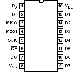
CDP68HC68P1: Features: • Fully Static Operation• Operating Voltage Range 3-6V• Compatible with Intersil/Motorola SPI Bus• 2 External Address Pins Tied to VDD or VSS to Allow Up to 4 Devic...

floor Price/Ceiling Price

Part Number:
CDP68HC68P1
Supply Ability:
5000

Price Break

  • Qty
  • 1~5000
  • Unit Price
  • Negotiable
  • Processing time
  • 15 Days
Total Cost: $ 0.00

SeekIC Buyer Protection PLUS - newly updated for 2013!

  • Escrow Protection.
  • Guaranteed refunds.
  • Secure payments.
  • Learn more >>

Month Sales

268 Transactions

Rating

evaluate  (4.8 stars)

Upload time: 2024/3/27

Payment Methods

All payment methods are secure and covered by SeekIC Buyer Protection PLUS.

Notice: When you place an order, your payment is made to SeekIC and not to your seller. SeekIC only pays the seller after confirming you have received your order. We will also never share your payment details with your seller.
Product Details

Description


Features:

• Fully Static Operation
• Operating Voltage Range 3-6V
• Compatible with Intersil/Motorola SPI Bus
• 2 External Address Pins Tied to VDD or VSS to Allow Up to 4 Devices to Share the Same Chip Enable
• Versatile Bit-Set and Bit-Clear Capability
• Accepts Either SCK Clock Polarity - SCK Voltage Level is Latched When Chip Enable Goes Active
• All Inputs are Schmitt-Trigger
• 8-Bit I/O Port - Each Bit can be Individually Programmed as an Input or Output Via an 8-Bit Data Direction Register
• Programmable On Board Comparator
• Simultaneous Transfer of Compare Information to CPU During Read or Write - Separate Access Not Required


Pinout

  Connection Diagram


Specifications

DC Supply Voltage Range, (VDD) . . . . . . . . . . . . . .. . . -0.5V to +7V
   (Voltage Referenced to VSS Terminal)
Input Voltage Range, All Inputs . . . . . . . . . ... . -0.5V to VDD +0.5V
DC Input Current, Any One Input . . . . . . . . . . . .  .. . . . . . . ±10mA
Power Dissipation Per Package (PD)
   TA = -40oC to 60oC (Package Type E) . . . . . . . . . . . . . . .500mW
   TA = 60oC to 85oC (Package Type E)
   Derate Linearly at . . . . . . . . . . . . . . . . . . . 12mW/oC to 200mW
   TA = -40oC to 60oC (Package Type M) (Note 1) .  . oC. . .300mW
   TA = 60oC to 85oC (Package Type M) (Note 1)
   Derate Linearly at . . . . . . . . . . . . . . . . . .  . . 5mW/oC to 175mW


Description

The CDP68HC68P1 is a serially addressed 8-bit Input/Output port that allows byte or individual bit control. CDP68HC68P1 consists of three registers, an output buffer and control logic. Data is shifted in and out of the device via shift register that utilizes the SPI (Serial Peripheral Interface) bus. The I/O port data flow is controlled by the Data Direction Register and data is stored in the Data Register that outputs or senses the logic levels at the buffered I/O pins. All inputs, including the serial interface are Schmitt triggered. CDP68HC68P1 also features a compare function that compares the data register and port pin values for 4 programmable conditions and sets a software accessible flag if the condition is satisfied. The user also has the option of bit-set or bit-clear when writing to the data register.


Customers Who Bought This Item Also Bought

Margin,quality,low-cost products with low minimum orders. Secure your online payments with SeekIC Buyer Protection.
Optical Inspection Equipment
Line Protection, Backups
Programmers, Development Systems
Batteries, Chargers, Holders
Static Control, ESD, Clean Room Products
Computers, Office - Components, Accessories
View more