Features: `SDTV/HDTV serial digital video standard compliant
`Supports 270 Mbps, 360 Mbps, 540 Mbps, 1.4835Gbps and 1.485 Gbps SDV data rates with auto-detection
`LSB dithering option
`No external serial data rate setting or VCO filtering components required*
`Fast PLL lock time: < 150µs typical at 1.485 Gbps
`Adjustable depth video FIFO for timing alignment
`Built-in self-test (BIST) and video test pattern generator (TPG)*
`Automatic EDH/CRC word and flag generation and insertion
`On-chip ancilliary data FIFO and insertion control circuitry
`Flexible control and configuration I/O port
`LVCMOS compatible data and control inputs and outputs
`75W ECL-compatible, differential, serial cable-driver outputs
`3.3V I/O power supply, 2.5V logic power supply operation
`Low power: typically 430mW
`64-pin TQFP package
`Commercial temperature range 0 to +70
* Patent applications made or pending.
Application`SDTV/HDTV parallel-to-serial digital video interfaces for:
- Video cameras
- VTRs
- Telecines
- Digital video routers and switchers
- Digital video processing and editing equipment
- Video test pattern generators and digital video test equipment
- Video signal generatorsPinout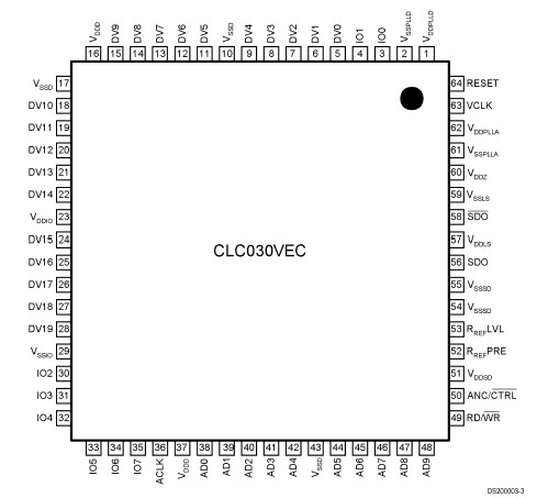 Specifications
| Max Data Rate |
1485 Mbps |
| SupplyVoltage |
3.3 Volt |
| OtherSupply Voltage |
2.5V |
| Integrated Cable Driver |
Yes |
| External VCO Required |
Yes |
| Parallel Interface |
10/20-bit LVDS/ECL |
| Power Consumption_ |
430 mW |
| Temperature Min |
0 deg C |
| Temperature Max |
70 deg C |
| Rise/Fall Times |
200 ps |
| Supply Current |
66 mA |
| OtherSupply Current |
85 mA |
| Output Swing |
0.8 Volt |
| Function |
Serializer |
| View Using Catalog |
CMOS I/O Supply Voltage
(VDDIOVSSIO): 4.0V
SDO Supply Voltage
(VDDSDVSSSD): 4.0V
Digital Logic Supply Voltage
(VDDDVSSD): 3.0V
PLL Supply Voltage
(VDDPLLVSSPLL): 3.0V
CMOS Input Voltage VSSIO -0.15V to
(Vi): VDDIO +0.15V
CMOS Output Voltage VSSIO +0.15V to
(Vo): VDDIO +0.15V
CMOS Input Current (single input):
Vi = VSSIO -0.15V: -5 mA
Vi = VDDIO +0.15V: +5 mA
CMOS Output Source/Sink Current:±10 mA
SDO Output Sink Current:40 mA
Package Thermal Resistance
JA @ 0 LFM Airflow47/W
JA @ 500 LFM Airflow27/W
JC6.5/W
Storage Temp. Range:-65 to +150
Junction Temperature: +150
Lead Temperature (Soldering 4 Sec): +260
ESD Rating (HBM): 2 kV
ESD Rating (MM): 250VDescriptionThe CLC030 SMPTE 292M/259M Digital Video Serializer with Ancilliary Data FIFO and Integrated Cable Driver is a monolithic integrated circuit that encodes, serializes and transmits bit-parallel digital video data conforming to SMPTE 125M and 267M standard definition, 10-bit wide component video and SMPTE 260M, 274M, 295M and 296M highdefinition, 20-bit wide component video standards. The CLC030 operates at SMPTE 259M serial data rates of 270 Mbps, 360 Mbps, the SMPTE 344M (proposed) serial data rate of 540 Mbps; and the SMPTE 292M serial data rates of 1483.5 and 1.485 Gbps. The serial data clock frequency is internally generated and requires no external frequency setting, trimming or filtering components*.
Functions performed by the CLC030 include: parallel-toserial data conversion, SMPTE standard data encoding, NRZ to NRZI data format conversion, serial data clock generation and encoding with the serial data, automatic video rate and format detection, ancilliary data packet storage, manipulation and insertion, and serial data output driving.
The CLC030 has circuitry for automatic EDH/CRC character and flag generation and insertion per SMPTE RP-165 (standard definition) or SMPTE 292M (high definition). Optional LSB dithering is implemented which prevents pathological pattern generation. Unique to the CLC030 are its video and ancilliary data FIFOs. The video FIFO allows from 0 to 4 parallel data clock delays to be inserted in the data path for video timing purposes. The ancilliary data port and on-chip FIFO and control circuitry offer elegant handling and insertion of ancilliary data packets and checksums in the ancilliary data space. The CLC030 also has an exclusive built-in selftest (BIST) and video test pattern generator (TPG) with SD and HD component video test patterns: reference black, PLL and EQ pathologicals and colour bars in 4:3 and 16:9 raster formats for NTSC and PAL standards*. The colour bar patterns feature optional bandwidth limiting coding in the chroma and luma transitions.
The CLC030 has a unique multi-function I/O port which provides access to control and configuration signals and data. This port may be programmed to provide external access to control functions and data for use as inputs and outputs. This allows the designer greater flexibility in tailoring the CLC030 to the desired application. At power-up or after a reset command, the CLC030 is auto-configured to a default operating condition. Separate power pins for the output driver, PLL and the serializer improve power supply rejection, output jitter and noise performance.
The CLC030's internal circuitry is powered from +2.5V and the I/O circuitry from a +3.3V supply. Power dissipation is typically 430mW at 1.485Gbps including two 75W ACcoupled and back-matched output loads. The device is packaged in a 64-pin TQFP.

 CLC030 Data Sheet