CLC402

Features: 0.0025% settling in 25ns (32ns max)0.5mV input offset voltage, 3mV/°C drift±1 to ±8 closed-loop gain rangeLow power, 150mW0.01%/0.05° differential gain/phaseApplicationHigh-accuracy A/D systems (12-14 bits)High-accuracy D/A convertersHigh-speed communicationsIF processorsVideo distributi...

product image

CLC402 Picture
SeekIC No. : 004313706 Detail

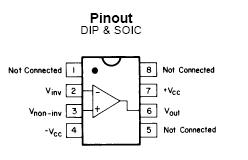
CLC402: Features: 0.0025% settling in 25ns (32ns max)0.5mV input offset voltage, 3mV/°C drift±1 to ±8 closed-loop gain rangeLow power, 150mW0.01%/0.05° differential gain/phaseApplicationHigh-accuracy A/D sy...
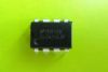
floor Price/Ceiling Price

Part Number:
CLC402
Supply Ability:
5000

Price Break

  • Qty
  • 1~5000
  • Unit Price
  • Negotiable
  • Processing time
  • 15 Days
Total Cost: $ 0.00

SeekIC Buyer Protection PLUS - newly updated for 2013!

  • Escrow Protection.
  • Guaranteed refunds.
  • Secure payments.
  • Learn more >>

Month Sales

268 Transactions

Rating

evaluate  (4.8 stars)

Upload time: 2024/4/30

Payment Methods

All payment methods are secure and covered by SeekIC Buyer Protection PLUS.

Notice: When you place an order, your payment is made to SeekIC and not to your seller. SeekIC only pays the seller after confirming you have received your order. We will also never share your payment details with your seller.
Product Details

Description


Features:

0.0025% settling in 25ns (32ns max)
0.5mV input offset voltage, 3mV/°C drift
±1 to ±8 closed-loop gain range
Low power, 150mW
0.01%/0.05° differential gain/phase


Application

High-accuracy A/D systems (12-14 bits)
High-accuracy D/A converters
High-speed communications
IF processors
Video distribution


Pinout

  Connection Diagram


Specifications

Gain Bandwidth 195 MHz
Slew Rate 800 Volts/usec
Input OutputType Not Rail to Rail
Supply Min 10 Volt
Supply Max 14 Volt
Channels 1 Channels
Supply Current Per Channel 15 mA
PowerWise Rating 2 76.9 uA/MHz
Offset Voltage max, 25C 1.6 mV
Max Input Bias Current 45000 nA
Output Current 55 mA
Voltage Noise 1.7 nV/root(Hz)
Shut down No
Feedback Type Current
Av+1 BW 177 MHz
Av+2 BW 195 MHz
Av+5 BW 150 MHz
Av+10 BW 100 MHz
Av+20 BW 60 MHz
HD 2nd -50 dB
HD 3rd -60 dB
Diff Gain 0.01 dB
Diff Phase 0.05 %
Settling Time 10 ns
Tsettling Conditions to 0.1%
Special Features Undefined
Function Op Amp
Temperature Min -40 deg C
Temperature Max 85 deg C
View Using Catalog


Description

The CLC402 is an operational amplifier designed for low-gain applications (±1 to ±8), requiring fast, accurate settling and superior DC accuracy. Settling to 0.0025% in 25ns (32ns guaranteed over temperature), the CLC402 is ideal as the input amplifier in high accuracy (up to 14-bits) A/D systems. Unlike most other high-speed op amps, the CLC402 is free of thermally induced tails in the settling response.

The CLC402 is an upgrade to and pin compatible with the industry standard CLC400. Constructed using a unique, proprietary design and an advanced complementary bipolar process, it offers performance far beyond ordinary monolithic op amps. In addition, unlike many other high-speed op amps, the CLC402 offers both high performance and stability without the need for compensation circuitry-even at a gain of +1.

Supporting the CLC402's excellent pulse performance are improved DC characteristics. The CLC402's input offset voltage is typically 0.5mV and is guaranteed to be less than 1.6mV at +25°C. The input offset voltage drift is typically only 3µV/°C

Design Tools


Title Size in Kbytes Date
Amplifiers Selection Guide software for Windows 8 Kbytes 6-Mar-2007 View

If you have trouble printing or viewing PDF file(s), see Printing Problems.


Customers Who Bought This Item Also Bought

Margin,quality,low-cost products with low minimum orders. Secure your online payments with SeekIC Buyer Protection.
Sensors, Transducers
Transformers
Test Equipment
Fans, Thermal Management
Discrete Semiconductor Products
Batteries, Chargers, Holders
View more