Features: • Single 3.0 V read, program, and erase Minimizes system level power requirements
• Compatible with JEDEC-standard commands Uses same software commands as E2PROMs
• Compatible with JEDEC-standard world-wide pinouts
48-pin TSOP(I) (Package suffix: PFTN Normal Bend Type)
48-ball FBGA (Package suffix: PBT)
48-ball SCSP (Package suffix: PW)
• Minimum 100,000 program/erase cycles
• High performance 90 ns maximum access time
• Sector erase architecture
One 8K word, two 4K words, one 16K word, and fifteen 32K words sectors in word mode
One 16K byte, two 8K bytes, one 32K byte, and fifteen 64K bytes sectors in byte mode
Any combination of sectors can be concurrently erased. Also supports full chip erase
• Boot Code Sector Architecture B = Bottom sector
• Embedded EraseTM* Algorithms Automatically pre-programs and erases the chip or any sector
• Embedded ProgramTM* Algorithms Automatically writes and verifies data at specified address
• Data Polling and Toggle Bit feature for detection of program or erase cycle completion
• Ready/Busy output (RY/BY) Hardware method for detection of program or erase cycle completion
• Automatic sleep mode When addresses remain stable, automatically switch themselves to low power mode
• Low VCC write inhibit £ 2.5 V
• Erase Suspend/Resume Suspends the erase operation to allow a read in another sector within the same device
• Sector protection Hardware method disables any combination of sectors from program or erase operations
• Sector Protection set function by Extended sector Protect command
• Temporary sector unprotection Temporary sector unprotection via the RESET pinPinout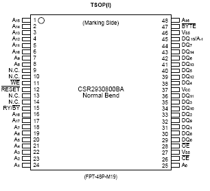 Specifications
| Parameter |
Symbol |
Rating |
Unit |
| Min |
Max |
| Storage Temperature |
|
55 |
+125 |
°C |
| Ambient Temperature with Power Applied |
|
40 |
+85 |
°C |
| Voltage with respect to Ground All pins except A9, OE, RESET *1 |
|
0.5 |
VCC+0.5 |
V |
| VCC *1 |
|
0.5 |
+5.5 |
V |
| A9, OE,, andRESET*2 |
|
0.5 |
+13.0 |
V |
DescriptionThe CSR2930800BA are a 8M-bit, 3.0 V-only Flash memory organized as 1M bytes of 8 bits each or 512K words of 16 bits each. TheCSR2930800BA are offered in a 48-pin TSOP(I), 44-pin SOP, and 48-ball FBGA packages. These devices are designed to be programmed in-system with the standard system 3.0 V VCC supply. 12.0 V VPP and 5.0 V VCC are not required for write or erase operations.
The devices can also be reprogrammed in standard EPROM programmers. The standard CSR2930800BA offer access times 90 ns, allowing operation of high-speed microprocessors without wait states. To eliminate bus contention the devices have separate chip enable (CE), write enable (WE), and output enable (OE) controls.
The CSR2930800BA are pin and command set compatible with JEDEC standard E2PROMs. Commands are written to the command register using standard microprocessor write timings. Register contents serve as input to an internal state-machine which controls the erase and programming circuitry. Write cycles also internally latch addresses and data needed for the programming and erase operations. Reading data out of the devices is similar to reading from 5.0 V and 12.0 V Flash or EPROM devices.
The CSR2930800BA are programmed by executing the program command sequence. This will invoke the Embedded Program Algorithm which is an internal algorithm that automatically times the program pulse widths and verifies proper cell margin. Typically, each sector can be programmed and verified in about 0.5 seconds. Erase is accomplished by executing the erase command sequence.
This will invoke the Embedded Erase Algorithm which is an internal algorithm that automatically preprograms the array if CSR2930800BA is not already programmed before executing the erase operation. During erase, the devices automatically time the erase pulse widths and verify proper cell margin.

 CSR2930800BA Data Sheet


