Features: General Modem Features
• V.90 data modem with receive rates up to 56k bps and send rates up to V.34 rates
− ITU-T V.90, K56flex, V.34 (33.6 kbps), V.32 bis, V.32, V.22 bis, V.22, V.23, and V.21; Bell 212A and 103
− V.42 LAPM and MNP 2-4 error correction
− V.42 bis and MNP 5 data compression
− V.250 and V.251 commands
• V.17 fax modem with send and receive rates up to 14.4 kbps
− V.17, V.29, V.27 ter, and V.21 channel 2
− EIA/TIA 578 Class 1 and T.31 Class 1.0 commands
• Telephony/TAM
− V.253 commands
− 8-bit -Law/A-Law coding (G.711)
− 8-bit/16-bit linear coding
− 8 kHz sample rate
− Concurrent DTMF, ring, and Caller ID detection
• V.80 synchronous access mode supports host-controlled communication protocols with H.324 interface support
• V.8/V.8bis and V.251 commands
• Cellular data hardware interface and software support (C models)
− Protocol stacks for PDC high speed data, PDC packet data, PHS data, CDMA IS-95A/IS-95B data, and GSM data
− API for customer-provided cellular data protocol stack
• Full-duplex Speakerphone (FDSP) Mode (S models)
− Microphone and speaker interface
− Telephone handset/headset interface
• Data/Fax/Voice call discrimination
• Host software/MMX-based digital signal processing
• Single configuration profile stored in host
• Operates in U.S./Japan/Canada
• Worldwide operation including U.S./Japan/Canada (W models)
− Complies to TBR21 and other country requirements
− Caller ID detection
• System compatibility
− Windows 95/98, Windows NT 4.0, Windows 2000, and Windows Millennium (Windows Me) operating systems
− Microsoft'/Intel PC 99 Windows Hardware Designer's Guide-compliant
− Advanced Configuration and Power Interface (ACPI)
− Unimodem/V compliant
− Pentium 166 MHz MMX-compatible PC or greater
− 16 Mbyte RAM or more
• Thin packages support low profile designs
− CX11250 HSD: 100-pin TQFP (1.2 mm max. height)
− CX20463 LSD: 32-pin TQFP (1.6 mm max. height)
− CX20437 VC: 32-pin TQFP (1.6 mm max. height)
• +3.3V operation with +5V tolerant digital inputs
PCI Bus Host Interface Features
• 32-bit PCI Bus host interface
− Meets PCI Local Bus Specification Rev. 2.2
− PCI Bus Mastering interface
− 33 MHz PCI clock support
• Supports Power Management
− Meets PCI Bus Power Management Spec. Rev. 1.1
− ACPI Power Management Registers
− APM support
− PME# support
− Vaux/Vpci power switching support (-PCI model option)
− VauxDET support
SmartDAA Features
• Digital PBX line protection
• System side powered DAA operates under poor line current supply conditions
• Wake-on-ring
• Ring detection
• Line polarity reversal detection
• Line current loss detection
• Caller ID (CID) detect
• Pulse dialing
• Line-in-use detection detects even while on-hook
• Remote hang-up detect for efficient call termination
• Extension pickup detect
• Call waiting detection
• Meets worldwide DC VI Masks requirements (W models)Application• Laptop, notebook, and handheld computers
• PCI Bus/Mini PCI embedded system boards
• PCI Bus/Mini PCI plug-in cardsPinout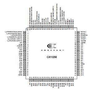 Specifications
| Parameter |
Symbol |
Limits |
Units |
| Supply Voltage |
VDD |
-0.5 to +4.0 |
VDC |
| Input Voltage |
VIN |
-0.5 to (VIO +0.5)* |
VDC |
| Storage Temperature Range |
TSTG |
-55 to +125 |
|
| Analog Inputs |
VIN |
-0.3 to (MAVDD + 0.5) |
VDC |
| Voltage Applied to Outputs in High Impedance (Off)State |
VHZ |
-0.5 to (VIO +0.5)* |
VDC |
| DC Input Clamp Current |
IIK |
±20 |
mA |
| DC Output Clamp Current |
IOK |
±20 |
mA |
| Static Discharge Voltage (25) |
VESD |
±2500 |
VDC |
| Latch-up Current (25) |
ITRIG |
±400 |
mA |
| * VIO = +3.3V ± 0.3V or +5V ± 5%. |
Caution: Handling CMOS Devices These devices contain circuitry to protect the inputs against damage due to high static voltages. However, it is advised that normal precautions be taken to avoid application of any voltage higher than maximum rated voltage. An unterminated input can acquire unpredictable voltages through coupling with stray capacitance and internal cross talk.
Both power dissipation and device noise immunity degrades. Therefore, all inputs should be connected to an appropriate supply voltage.
Input signals should never exceed the voltage range from 0.5V or more negative than GND to 0.5V or more positive than VDD. This prevents forward biasing the input protection diodes and possibly entering a latch up mode due to high current transients.
DescriptionCX11250 Modem operation, including dialing, call progress, telephone line interface, telephone handset interface, PDC HighSpeed/GSM interface, voice/speakerphone interface, and host interface functions are supported and controlled hrough the V.250, V.251, and V.253-compatible command set.
CX11250 modem hardware connects to the host processor via a PCI/Mini PCI bus interface. The OEM adds a crystal circuit,
EEPROM, DIB and LSD power rectifier and filter components, telephone line interface, optional telephone handset interface, optional PDC high speed/GSM interface, optional voice/speakerphone interface, and other supporting iscrete components as required by the modem model and the application to complete the system.

 CX11250 Data Sheet