SeekIC No. : 004318062
Detail
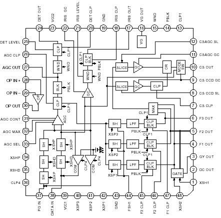
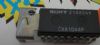
CXA1390AR: Features: • Pin compatible upgraded version of CXA1390Q/R which can be swapped out while using same peripheral chips• Almost completely corrects irregular pulses and their negative affec...
 CXA1390AR Data Sheet
floor Price/Ceiling Price
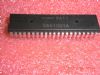
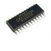
- Part Number:
- CXA1390AR
- Supply Ability:
- 5000
Price Break
- Qty
- 1~5000
- Unit Price
- Negotiable
- Processing time
- 15 Days
SeekIC Buyer Protection PLUS - newly updated for 2013!
- Escrow Protection.
- Guaranteed refunds.
- Secure payments.
- Learn more >>
Month Sales
268 Transactions
Payment Methods
All payment methods are secure and covered by SeekIC Buyer Protection PLUS.
Notice: When you place an order, your payment is made to SeekIC and not to your seller. SeekIC only pays the seller after confirming you have received your order. We will also never share your payment details with your seller.