Features: R-R Mode R-L, R-FT Modes **DC Mode**
• Fast Cycle/Access Time tKHKH / tKHQV tKHKH / tKHQV tKHKH / tKHQV
CXK77B1840 -4A 4.0ns / 2.3ns 4.8ns / 4.8ns 4.0ns / 5.2ns
-4 4.0ns / 2.3ns 5.3ns / 5.3ns 4.0ns / 5.2ns
-45A 4.0ns / 2.3ns 5.3ns / 5.3ns 4.5ns / 6.0ns
-45 5.0ns / 2.5ns 6.5ns / 6.5ns 4.5ns / 6.5ns
Note: Contact Sony Memory Marketing for availability of DC mode functionality.
• 4 synchronous modes of operation, selectable by mode pins:
Register-Register; Register-Latch; Register-Flow Thru; Dual Clock
• Single +3.3V power supply: 3.3V ± 5%
• Dedicated output supply voltage: VDDQ (1.5V typical)
• Inputs and outputs are HSTL / extended HSTL compatible.
• Differential clock input (K/K, C/C).
• All inputs (except asynchronous G and ZZ) and outputs are registered on a single clock edge.
• Byte Write capability.
• Late Write scheme to eliminate one dead cycle from Read-to-Write transitions.
• Self-timed write cycles.
• Sleep (power down) mode.
• JTAG boundary scan (subset of IEEE standard 1149.1).
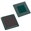
• 119 pin (7x17) Plastic Ball Grid Array (PBGA) package.Specifications
| Item |
Symbol |
Rating |
Unit |
| Supply voltage |
VDD |
0.5 to +4.6 |
V |
| Output Supply Voltage |
VDD |
0.5 to +4.6 |
V |
| Input voltage |
VIN |
-0.5 to VDD+0.5 (4.6V max.) |
V |
| Output Supply Voltage |
VOUT |
-0.5 to VDDQ+0.5 (4.6V max.) |
V |
| Operating temperature |
TA |
0 to 85 |
|
| Junction Temperature |
TJ |
0 to +110 |
|
| Storage temperature |
TSTG |
-55 to 150 |
|
(1)Stresses greater than those listed under "Absolute Maximum Ratings" may cause permanent damage to the device. This is a stress rating only, and functional operation of the device at these or any other conditions other than those indicated in the operational sections of this specification is not implied. Exposure to absolute maximum rating conditions for extended periods may affect reliability.DescriptionThe CXK77B1840GB is a high speed BiCMOS synchronous static RAM with common I/O pins, organized as 262,144-words by 18-bits. This synchronous SRAM integrates input registers, high speed RAM, output registers/latches, and a one-deep write buffer onto a single monolithic IC. Four different read protocols - Register-Register (R-R), Register-Latch (R-L), Register-Flow Thru (R-FT), and Dual Clock (DC), and an enhanced write protocol - Late (Delayed) Write (LW), are supported, providing a flexible, high-performance user interface.
All input signals except G (Output Enable) and ZZ (Sleep Mode) CXK77B1840GB are registered on the positive edge of K clock.
Read cycles can be controlled in one of four ways - with registered outputs in Register-Register mode, with latched outputs in Register-Latch mode, with flow-through outputs in Register-Flow Thru mode, or with registered outputs using a dedicated output control clock (C clock) in Dual Clock mode. The read protocol is user-selectable through external mode pins M1 and M2.
Write cycles follow a Late Write protocol, where data CXK77B1840GB is provided to the SRAM one clock cycle after the address and control signals, eliminating one dead cycle from Read-to-Write transitions. In this scheme, when a write cycle is initiated, the address and data stored in the SRAM's write buffer during the previous write cycle are directed to the SRAM's memory core, while, simultaneously, the address and data from the current write cycle are stored in the SRAM's write buffer. In both Register-Latch and Register-Flow Thru modes, when SW (Global Write Enable) is driven active, the subsequent positive edge of K clock tristates the SRAM's output drivers immediately, allowing consecutive Read-Write-Read operations. The write cycle is internally self-timed, which eliminates complex off-chip write pulse generation and provides increased flexibility for incoming signals.
The output drivers CXK77B1840GB are series terminated, and the output impedance is programmable through an external impedance matching resistor RQ. By connecting RQ between ZQ and VSS, the output impedance of all 18 DQ pins can be precisely controlled.
Sleep (power down) mode control CXK77B1840GB is provided through the asynchronous ZZ input. 250 MHz operation is obtained rom a single 3.3V power supply. JTAG boundary scan interface is provided using a subset of IEEE standard 1149.1 protocol.

 CXK77B1840GB Data Sheet