CXK77K18R320GB

Features: • 3 Speed Bins Cycle Time / Access Time -3 3.0ns / 1.6ns -33 3.3ns / 1.6ns-4 4.0ns / 2.0ns• Single 1.8V power supply (VDD): 1.8V ± 0.1V Note: 2.5V VDD is also supported. Please contact Sony Memory Marketing Department for further information.• Dedicated output supply vo...

product image

CXK77K18R320GB Picture
SeekIC No. : 004318733 Detail

CXK77K18R320GB: Features: • 3 Speed Bins Cycle Time / Access Time -3 3.0ns / 1.6ns -33 3.3ns / 1.6ns-4 4.0ns / 2.0ns• Single 1.8V power supply (VDD): 1.8V ± 0.1V Note: 2.5V VDD is also supported. Please...

floor Price/Ceiling Price

Part Number:
CXK77K18R320GB
Supply Ability:
5000

Price Break

  • Qty
  • 1~5000
  • Unit Price
  • Negotiable
  • Processing time
  • 15 Days
Total Cost: $ 0.00

SeekIC Buyer Protection PLUS - newly updated for 2013!

  • Escrow Protection.
  • Guaranteed refunds.
  • Secure payments.
  • Learn more >>

Month Sales

268 Transactions

Rating

evaluate  (4.8 stars)

Upload time: 2024/4/23

Payment Methods

All payment methods are secure and covered by SeekIC Buyer Protection PLUS.

Notice: When you place an order, your payment is made to SeekIC and not to your seller. SeekIC only pays the seller after confirming you have received your order. We will also never share your payment details with your seller.
Product Details

Description


Features:

3 Speed Bins     Cycle Time / Access Time
       -3                              3.0ns / 1.6ns
       -33                            3.3ns / 1.6ns
       -4                              4.0ns / 2.0ns
• Single 1.8V power supply (VDD): 1.8V ± 0.1V
   Note: 2.5V VDD is also supported. Please contact Sony Memory Marketing Department for further information.
• Dedicated output supply voltage (VDDQ): 1.5V to 1.8V typical
• HSTL-compatible I/O interface with dedicated input reference voltage (VREF): VDDQ/2 typical
• Register - Register (R-R) read protocol
• Late Write (LW) write protocol
• Full read/write coherency
• Byte Write capability
• Differential input clocks (K/K)
• Asynchronous output enable (G)
• Sleep (power down) mode via dedicated mode pin (ZZ)
• Programmable output driver impedance
• JTAG boundary scan (subset of IEEE standard 1149.1)
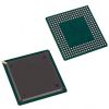
• 119 pin (7x17), 1.27mm pitch, 14mm x 22mm Ball Grid Array (BGA) package


Specifications

Parameter
Symbol
Rating
Units
Supply Voltage
VDD
-0.5 to +2.5
V
Output Supply Voltage
VDDQ
-0.5 to +2.3
V
Input Voltage (Address, Control, Data, Clock)
VIN
-0.5 to VDDQ + 0.5 (2.3V max)
V
Input Voltage (M1, M2)
VMIN
-0.5 to VDD + 0.5 (2.5V max)
V
Input Voltage (TCK, TMS, TDI)
VTIM
-0.5 to VDD + 0.5 (2.5V max)
V
Operating Temperature
TA
0 to 85
Junction Temperature
TJ
0 to 110
Storage Temperature
TSTG
-55 to 150
Notes: Stresses greater than those listed under "Absolute Maximum Ratings" may cause permanent damage to the device. This is a stress rating only, and functional operation of the device at these or any other conditions other than those indicated in the operational sections of this specification is not implied. Exposure to absolute maximum rating conditions for extended periods may affect reliability.


Description

The CXK77K18R320GB is a high speed CMOS synchronous static RAM with common I/O pins, organized as 2,097,152 words by 18 bits. This synchronous SRAMs integrates input registers, high speed RAM, output registers, and a one-deep write buffer onto a single monolithic IC. Register - Register (R-R) read operations and Late Write (LW) write operations are supported, providing a high-performance user interface.

All address and control input signals CXK77K18R320GB except G (Output Enable) and ZZ (Sleep Mode) are registered on the rising edge of the K differential input clock.

During read operations, output data is driven valid from the rising edge of K, one full clock cycle after the address is registered.

During write operations, input data is registered on the rising edge of K, one full clock cycle after the address is registered.

Sleep (power down) capability CXK77K18R320GB is provided via the ZZ input signal.

Output drivers CXK77K18R320GB are series terminated, and output impedance is programmable via the ZQ input pin. By connecting an external control resistor RQ between ZQ and VSS, the impedance of the output drivers can be precisely controlled.

333 MHz operation CXK77K18R320GB is obtained from a single 1.8V power supply. JTAG boundary scan interface is provided using a subset of IEEE standard 1149.1 protocol.


Customers Who Bought This Item Also Bought

Margin,quality,low-cost products with low minimum orders. Secure your online payments with SeekIC Buyer Protection.
Power Supplies - Board Mount
Industrial Controls, Meters
Memory Cards, Modules
View more