Features: • 4 Speed Bins Cycle Time / Access Time
-4 (-4A) (-4B) 4.0ns / 3.9ns (3.8ns) (3.7ns)
-42 (-42A) (-42B) 4.2ns / 4.2ns (4.1ns) (4.0ns)
-43 (-43A) (-43B) 4.3ns / 4.5ns (4.4ns) (4.3ns)
-44 4.4ns / 4.7ns
• Single 3.3V power supply (VDD): 3.3V ± 5%
• Dedicated output supply voltage (VDDQ): 1.9V typical
• HSTL-compatible I/O interface with dedicated input reference voltage (VREF): 0.85V typical
• Register - Latch (R-L) read operations
• Late Write (LW) write operations
• Conventional 16Mb or Error-Correcting (EC) 8Mb mode of operation, selectable via dedicated mode pin (M2)
• Full read/write coherency
• Byte Write capability
• One cycle deselect
• Differential input clocks (K/K)
• Programmable impedance output drivers
• Sleep (power down) mode via dedicated mode pin (ZZ)
• JTAG boundary scan (subset of IEEE standard 1149.1)
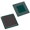
• 119 pin (7x17), 1.27mm pitch, 14mm x 22mm Ball Grid Array (BGA) packageSpecifications
| Item |
Symbol |
Rating |
Unit |
| Supply voltage |
VDD |
-0.5 to +3.8 |
V |
| Output Supply Voltage |
VDDQ |
-0.5 to +2.3 |
V |
| Input Voltage (Address, Control, Data, Clock) |
VIN |
-0.5 to VDDQ + 0.5 |
V |
| Input Voltage (M1, M2) |
VMIN |
-0.5 to VDD + 0.5 (3.8V max.) |
V |
| Input Voltage (TCK, TMS, TDI)) |
VTIN |
-0.5 to +3.8V |
W |
| Operating Temperature |
TA |
0 to 85 |
°C |
| Junction Temperature |
TJ |
0 to 110 |
°C |
| Storage Temperature |
TSTG |
-55 to 150 |
°C |
DescriptionThe CXK77P36E160GB (organized as 524,288 words by 36 bits) and the CXK77P18E160GB (organized as 1,048,576 words by 18 bits) are high speed CMOS synchronous static RAMs with common I/O pins. These synchronous SRAMs integrate input registers, high speed RAM, output latches, and a one-deep write buffer onto a single monolithic IC. Register - Latch (R-L) read operations and Late Write (LW) write operations are supported, providing a high-performance user interface.
Two distinct R-L modes of operation CXK77P36E160GB are supported, selectable via the M2 mode pin. When M2 is "high", these devices function as conventional 16Mb R-L SRAMs, and pin 2B functions as a conventional SA address input. When M2 is "low", these devices function as Error-Correcting (EC) 8Mb R-L SRAMs, and pin 2B is ignored.
When Error-Correcting 8Mb R-L mode CXK77P36E160GB is selected, the SRAM is divided into two banks internally - a "primary" bank and a"secondary" bank. During write operations, input data is ultimately written to both banks internally (through one stage of write pipelining). During read operations, data is read from both banks internally, and each byte of primary bank data is individually parity-checked. If the parity of a particular byte of primary data is correct (that is, "odd"), it is driven valid externally. If the parity of a particular byte of primary data is incorrect (that is, "even"), it is discarded, and the corresponding byte of secondary bank data is driven valid externally. Primary / secondary bank data selection is performed on each data byte independently.
Data read from the secondary bank CXK77P36E160GB is NOT parity-checked.
Data read from the write buffer is NOT parity-checked.
All address and control input signals except ZZ (Sleep Mode) are registered on the rising edge of K (Input Clock).
During read operations, output data is driven valid from the falling edge of K, one half clock cycle after the address is registered.
During write operations, input data CXK77P36E160GB is registered on the rising edge of K, one full clock cycle after the address is registered.
The output drivers CXK77P36E160GB are series terminated, and the output impedance is programmable through an external impedance matching resistor RQ. By connecting RQ between ZQ and VSS, the output impedance of all DQ pins can be precisely controlled. Sleep (power down) mode control is provided through the asynchronous ZZ input. 250 MHz operation is obtained from a single 3.3V power supply. JTAG boundary scan interface is provided using a subset of IEEE standard 1149.1 protocol.

 CXK77P36E160GB Data Sheet


