Features: • 3 Speed Bins Cycle Time / Data Access Time
-33 3.3ns / 1.8ns
-4 4.0ns / 2.1ns
-5 5.0ns / 2.3ns
• Single 1.8V power supply (VDD): 1.7V (min) to 1.95V (max)
• Dedicated output supply voltage (VDDQ): 1.4V (min) to VDD (max)
• HSTL-compatible I/O interface with dedicated input reference voltage (VREF): VDDQ/2 typical
• Common I/O
• Double Data Rate (DDR) data transfers
• Pipelined (PL) read operations
• Late Write (LW) write operations
• Burst capability with internally controlled Linear Burst address sequencing
• Burst length of two or four, with automatic address wrap
• Full read/write data coherency
• Differential input clocks (CK and CK)
• Data-referenced output clocks (CQ1, CQ1, CQ2, CQ2)
• Programmable output driver impedance via dedicated control pin (ZQ)
• Depth expansion capability (2 or 4 banks) via programmable chip enables (E2, E3, EP2, EP3)
• JTAG boundary scan (subset of IEEE standard 1149.1)
• 209 pin (11x19), 1mm pitch, 14mm x 22mm Ball Grid Array (BGA) packagePinout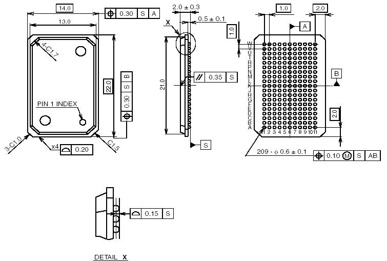 Specifications
| Parameter |
Symbol |
Rating |
Unit |
| Supply voltage |
VDD |
-0.5 to +2.5 |
V |
| Output Supply Voltage |
VDDQ |
-0.5 to +2.3 |
Input Voltage (Address, Control, Data, Clock)
(MCL pins 3B, 8B, 4C, 9C, 6W) |
VIN |
-0.5 to VDDQ+0.5 (2.3V max) |
Input Voltage (EP2, EP3)
(MCH pins 6J, 6M, 6N)
(MCL pins 6D, 6K, 6L, 6P, 6T) |
VMIN |
-0.5 to VDD+0.5 (2.5V max) |
W |
| Input Voltage (TCK, TMS, TDI) |
VTIN |
-0.5 to VDD+0.5 (2.5V max) |
°C |
| Operating Temperature |
TA |
0 to 85 |
| Junction Temperature |
TJ |
0 to 110 |
| Storage Temperature |
TSTG |
-55 to 150 |
°C |
DescriptionThe CXK79M36C162GB is a high speed CMOS synchronous static RAM with common I/O pins. It is manufactured in compliance with the JEDEC-standard 209 pin BGA package pinout defined for SigmaRAM™ devices. It integrates input registers, high speed RAM, output registers, and a two-deep write buffer onto a single monolithic IC. Double Data Rate (DDR) Pipelined(PL) read operations and LateWrite (LW) write operations are supported, providing a high-performance user interface. Positive and negative output clocks are provided for applications requiring source synchronous operation.
All address and control input signals CXK79M36C162GB are registered on the rising edge of the CK differential input clock. During read operations, output data is driven valid twice, from both the rising and falling edges of CK, beginning one full cycle after the address and control signals are registered.
During write operations CXK79M36C162GB, input data is registered twice, on both the rising and falling edges of CK, beginning one full cycle after the address and control signals are registered.
Because two pieces of data are always transferred during read and write operations, the least significant address bit of the internal memory array is not available as an external address pin to this device. Consequently, the number of external address pins available to the device is one less than the specified depth of the device (i.e. the 512Kb x 36 device has 18, not 19, external address pins). And, the user cannot choose the order in which the two pieces of data are read. Read data is always provided in the same order in which it is written.
Output drivers CXK79M36C162GB are series-terminated, and output impedance is programmable via the ZQ control pin.When an external resistor RQ is connected between ZQ and VSS, the impedance of the SRAM's output drivers is set to ~RQ/5.
300 MHz operation (600 Mbps) CXK79M36C162GB is obtained from a single 1.8V power supply. JTAG boundary scan interface is provided using a subset of IEEE standard 1149.1 protocol.

 CXK79M36C162GB Data Sheet