Features: • Wide-range instruction system (213 instructions) to cover various types of data.
- 16-bit arithmetic/multiplication and division/Boolean bit operation instructions
• Minimum instruction cycle 400ns at 10MHz operation 122µs at 32kHz operation
• Incorporated PROM capacity 24K bytes
• Incorporated RAM capacity 704 bytes (including fluorescent display area)
• Peripheral functions
- A/D converter 8-bit, 8-channel, successive approximation method(Conversion time of 32µs/10MHz)
- Serial interface SIO with 8-bit, 8-stage FIFO incorporated for data use (Auto transfer for 1 to 8 bytes), 1 channel 8-bit standard SIO, 1 channel
- Timer 8-bit timer, 8-bit timer/counter, 19-bit time base timer 16-bit capture timer/counter, 32kHz timer/counter
- Fluorescent display tube controller/driver Maximum of 384 segment display possible 1 to 16-digit dynamic display Dimmer function High voltage drive output (40V) Incorporated pull-down resistor Hardware key scan function Maximum of 16 *8 key matrix compatible
- Remote control reception circuit Incorporated noise elimination circuit Incorporated 8-bit, 6-stage FIFO for measurement data
- PWM output circuit 14 bits, 1 channel
- CTL duty detection circuit
- High-speed output circuit Precision of 800ns at 10MHz, 4 outputs.
• Interruption 19 factors, 15 vectors, multi-interruption possible
• Standby mode Sleep/stop
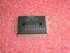
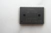
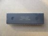
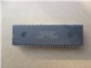
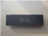
• Package 100-pin plastic QFPPinout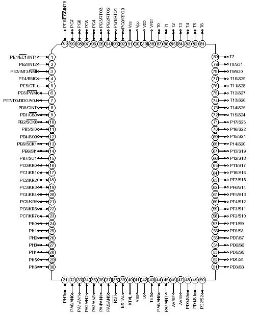 Specifications
| Item |
Symbol |
Rating |
Unit |
Remarks |
| Supply voltage |
VDD |
0.3 to +7.0 |
V |
|
| Vpp |
0.3 to +13.0 |
V |
Incorporated PROM |
| AVSS |
0.3 to +0.3 |
V |
|
| Input voltage |
VIN |
0.3 to +7.0*1 |
V |
|
| Output voltage |
VOUT |
0.3 to +7.0*1 |
V |
As P channel transistor is open drain,
VDD is reference. |
| Display output voltage |
VOD |
VDD 40 to VDD + 0.3 |
mA |
All pins excluding display outputs*2
(value per pin) |
| High level output current |
IOH |
5 |
mA |
Display outputs S0 to S23 (value per pin) |
| IODH1 |
15 |
mA |
Display outputs T0 to T7, and T8/S31 to
T15/S24 (value per pin) |
| IODH2 |
50 |
mA |
Total for all pins excluding display outputs |
| High level total output current |
IOH |
40 |
mA |
Total for all display outputs |
| IODH |
100 |
mA |
Port 1 |
| Low level output current |
IOL |
15 |
mA |
Large current Port 1 *3 |
| IOLC |
20 |
mA |
Total for all output pins |
| Operating temperature |
Topr |
20 to +75 |
°C |
|
| Storage temperature |
Tstg |
55 to +150 |
°C |
|
| Allowable power dissipation |
PD |
600 |
mW |
|
DescriptionThe CXP822P24 is a CMOS 8-bit single chip microcomputer integrating on a single chip an A/D converter, serial interface, timer/counter, time base timer, capture timer counter, fluorescent display tube controller/driver, remote control reception circuit, CTL duty detection circuit, 14-bit PWM output and highspeed output circuit besides the basic configurations of 8-bit CPU, PROM, RAM, and I/O port.
The CXP822P24 also provides sleep/stop function that enables lower power consumption.
CXP822P24 is the PROM-incorporated version of the CXP82224 with built-in mask ROM. This provides the additional feature of being able to write directly into the program. Thus, it is most suitable for evaluation use during system development and for smallquantity producton.

 CXP822P24 Data Sheet