CY2DP818-2

Features: • Low-voltage operation VDD = 3.3V• 1:8 fanout• Single-input-configurable for LVDS, LVPECL, or LVTTL• 8 pairs of LVPECL outputs with enable/disable• Drives a 50-ohm load• Low input capacitance• Low output skew• Low propagation delay Typical...

product image

CY2DP818-2 Picture
SeekIC No. : 004319293 Detail

CY2DP818-2: Features: • Low-voltage operation VDD = 3.3V• 1:8 fanout• Single-input-configurable for LVDS, LVPECL, or LVTTL• 8 pairs of LVPECL outputs with enable/disable• Drives a ...

floor Price/Ceiling Price

Part Number:
CY2DP818-2
Supply Ability:
5000

Price Break

  • Qty
  • 1~5000
  • Unit Price
  • Negotiable
  • Processing time
  • 15 Days
Total Cost: $ 0.00

SeekIC Buyer Protection PLUS - newly updated for 2013!

  • Escrow Protection.
  • Guaranteed refunds.
  • Secure payments.
  • Learn more >>

Month Sales

268 Transactions

Rating

evaluate  (4.8 stars)

Upload time: 2024/4/27

Payment Methods

All payment methods are secure and covered by SeekIC Buyer Protection PLUS.

Notice: When you place an order, your payment is made to SeekIC and not to your seller. SeekIC only pays the seller after confirming you have received your order. We will also never share your payment details with your seller.
Product Details

Description


Features:

• Low-voltage operation VDD = 3.3V
• 1:8 fanout
• Single-input-configurable for LVDS, LVPECL, or LVTTL
• 8 pairs of LVPECL outputs with enable/disable
• Drives a 50-ohm load
• Low input capacitance
• Low output skew
• Low propagation delay Typical (tpd < 4 ns)
• Industrial versions available
• Package available include: TSSOP
• Does not exceed Bellcore 802.3 standards
• Operation up to 350 MHz/700 Mbps


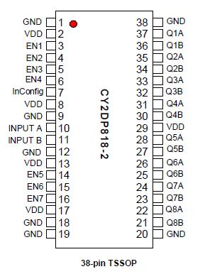
Pinout

  Connection Diagram


Specifications

Parameter Description Condition
Min.
Max.
Unit
VDD DC Supply Voltage Inputs and VCC
0.3
4.6
V
VDD DC Operating Voltage Outputs
0.3
VDD +0.3
V
VIN DC Input Voltage Relative to VSS, with or VDD applied
0.3
VDD +0.3
V
VOUT DC Output Voltage Relative to VSS
0.3
VDD + 0.9
V
VTT Output termination Voltage  
VDD ÷ 2
V
TS Temperature, Storage Non-functional
65
+150
°C
TA Temperature,Operating
Ambient
Commercial Functional
0
70
°C
Industrial Functional
40
+85
Multiple Supplies: The voltage on any input or I/O pin cannot exceed the power pin during power-up. Power supply sequencing is NOT required.


Description

This Cypress series of network circuits is produced using advanced 0.35-micron CMOS technology, achieving the industry's fastest logic.

The Cypress CY2DP818-2 fanout buffer features a single LVDS or a single-ended LVTTL-compatible input and eight LVPECL output pairs.

Designed for data-communications clock-management applications, the large fanout from a single input reduces loading on the input clock.

The CY2DP818-2 is ideal for both level translations from single-ended to LVPECL and/or for the distribution of LVPECL-based clock signals.

The Cypress CY2DP818-2 has configurable input functions.

The input is user-configurable via the Inconfig pin for single ended or differential input.


Customers Who Bought This Item Also Bought

Margin,quality,low-cost products with low minimum orders. Secure your online payments with SeekIC Buyer Protection.
Fans, Thermal Management
Connectors, Interconnects
Line Protection, Backups
Test Equipment
RF and RFID
Optical Inspection Equipment
View more