CY2V995

Features: • 2.5V or 3.3V operation• Split output bank power supplies• Output frequency range: 6 MHz to 200 MHz• Output-output skew: < 150 ps• Cycle-cycle jitter: < 100 ps• Selectable positive or negative edge synchronization• 8 LVTTL outputs driving ...

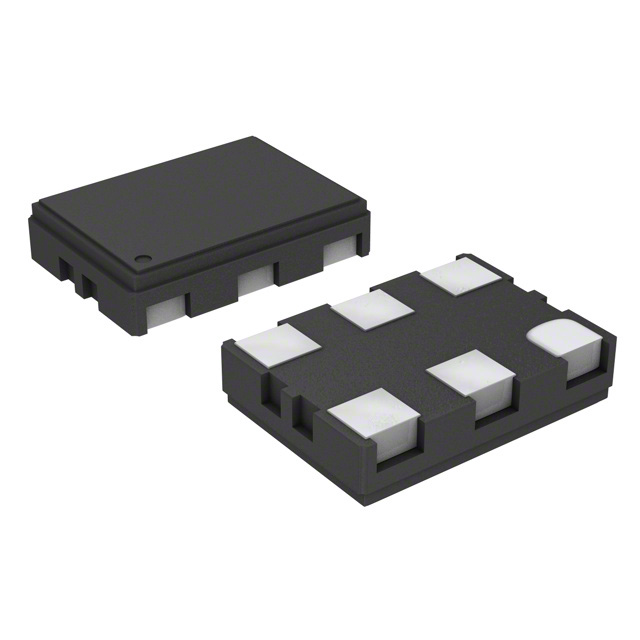
product image

CY2V995 Picture
SeekIC No. : 004319312 Detail

CY2V995: Features: • 2.5V or 3.3V operation• Split output bank power supplies• Output frequency range: 6 MHz to 200 MHz• Output-output skew: < 150 ps• Cycle-cycle jitter: <...

floor Price/Ceiling Price

Part Number:
CY2V995
Supply Ability:
5000

Price Break

  • Qty
  • 1~5000
  • Unit Price
  • Negotiable
  • Processing time
  • 15 Days
Total Cost: $ 0.00

SeekIC Buyer Protection PLUS - newly updated for 2013!

  • Escrow Protection.
  • Guaranteed refunds.
  • Secure payments.
  • Learn more >>

Month Sales

268 Transactions

Rating

evaluate  (4.8 stars)

Upload time: 2024/4/27

Payment Methods

All payment methods are secure and covered by SeekIC Buyer Protection PLUS.

Notice: When you place an order, your payment is made to SeekIC and not to your seller. SeekIC only pays the seller after confirming you have received your order. We will also never share your payment details with your seller.
Product Details

Description


Features:

• 2.5V or 3.3V operation
• Split output bank power supplies
• Output frequency range: 6 MHz to 200 MHz
• Output-output skew: < 150 ps
• Cycle-cycle jitter: < 100 ps
• Selectable positive or negative edge synchronization
• 8 LVTTL outputs driving 50Ω terminated lines
• LVCMOS/LVTTL over-voltage tolerant reference input
• Selectable phase-locked loop (PLL) frequency rangeand lock indicator
• (1-6,8,10,12)x multiply and (1/2,1/4)x divide ratios
• Spread-Spectrum-compatible
• Power-down mode
• Industrial temperature range: 40°C to +85°C
• 44-pin TQFP package


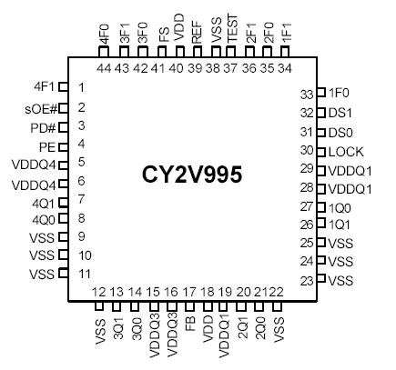
Pinout

  Connection Diagram


Specifications

Parameter Description Condition Min. Max. Unit
VDD Operating Voltage Functional% @ 2.5V ± 5 2.25 2.75 V
VDD Operating Voltage Functional @ 3.3V ± 10% 2.97 3.63 V
VIN(MIN) Input Voltage Relative to VSS VSS0.3 V
VIN(MAX) Input Voltage Relative to VDD VDD + 0.3 V
VREF(MAX) Reference Input Voltage VDD = 3.3V 5.5 V
VREF(MAX) Reference Input Voltage VDD = 2.5V 4.6 V
TS Temperature, Storage Non Functional 65 +150 °C
TA Temperature, Operating Ambient Functional 40 +85 °C
TJ Temperature, Junction Functional 155 °C
ESDHBM ESD Protection (Human Body Model) MIL-STD-883, Method 3015 2000 V
ØJC Dissipation, Junction to Case Mil-Spec 883E Method 1012.1 42 °C/W
ØJA Dissipation, Junction to Ambient JEDEC (JESD 51) 74 °C/W
UL-94 Flammability Rating @1/8 in. V 0
MSL Moisture Sensitivity Level 1
FIT Failure in Time Manufacturing Testing 10 ppm


Description

The CY2V995 is a low-voltage, low-power, eight output, 200-MHz clock driver. It features function necessary to optimize the timing of high-performance computer and communication systems.

The user can program the frequency of the output banks through nF[0:1] and DS[0:1] pins. Any one of the outputs can be connected to feedback input to achieve different reference frequency multiplication and divide ratios and zero input-output delay.

The device also features split output bank power supplies which enable the user to run two banks (1Qn and 2Qn) at apower supply level different from that of the other two banks (3Qn and 4Qn). Additionally, the PE pin controls the synchronizationof the output signals edge of the reference clock.


Customers Who Bought This Item Also Bought

Margin,quality,low-cost products with low minimum orders. Secure your online payments with SeekIC Buyer Protection.
Audio Products
Line Protection, Backups
Discrete Semiconductor Products
Cable Assemblies
Static Control, ESD, Clean Room Products
Test Equipment
View more