Features: •Low power, pin-compatible replacement for LCX and LPT families
•5V tolerant inputs and outputs
•24 mA balanced drive outputs
•Power-off disable outputs permits live insertion
•Edge-rate control circuitry for reduced noise
•FCT-C speed at 5.1 ns
•Latch-up performance exceeds JEDEC standard no. 17
•ESD > 2000V per MIL-STD-883D, Method 3015
•Typical output skew < 250 ps
•Industrial temperature range of 40to +85
•TSSOP (19.6-mil pitch) or SSOP (25-mil pitch)
•Typical Volp (ground bounce) performance exceeds Mil Std 883D
•VCC = 2.7V to 3.6V
Pinout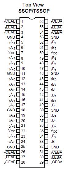 Specifications
(Above which the useful life may be impaired. For user
guidelines, not tested.)
Storage Temperature .................................................... -55to +125
Ambient Temperature with
Power Applied .............................................................. -55 to +125
Supply Voltage Range ..................................................... 0.5V to +4.6V
DC Input Voltage .............................................................-0.5V to +7.0V
DC Output Voltage ...........................................................-0.5V to +7.0V
DC Output Current
(Maximum Sink Current/Pin) ............................................-60 to +120 mA
Power Dissipation ............................................................................1.0W
Static Discharge Voltage...............................................................>2001V
(per MIL-STD-883, Method 3015)
DescriptionThe CY74FCT163543 is a 16-bit, high-speed, low power latched transceiver that is organized as two independent 8-bit D-type latched transceivers, containing twosets of eight D-type latches with separate LatchEnable (LEAB ,LEAB )and OutputEnable (LEAB ,LEAB )controls for each set to permit independent control of inputting and outputting in either direction of data flow. For data flow from A to B, for example, the A-to-B input Enable (CEAB) must be LOW in order to enter data from A or to take data fromB, as indicated in the truth table. With CAEB LOW, a LOWsignal on the A-to-B Latch Enable (LEAB) makes the A-to-B latches transparent; a subsequent LOW-to-HIGH transition of the LEAB signal puts the A latches in the storage mode andtheir outputsnolonger followtheAinputs. WithCEABandOEAB both LOW, the three-state B output buffers of CY74FCT163543 are active and reflect the data present at the output of the A latches. Control of data from B to A is similar, but usesCEAB, LEAB, and OEAB inputs.
The CY74FCT163543 has 24-mA balanced output drivers with current limiting resistors in the outputs. This reduces the need for external terminating resistors and provides for minimal undershoot and reduced ground bounce. The inputs and outputs are capable of being driven by 5.0V buses, allowing them to be used in mixed voltage systems as translators. The outputs of CY74FCT163543 are also designed with a power off disable feature enabling them to be used in applications requiring live insertion. Flow-through pinout and small shrink packaging simplify board design.

 CY74FCT163543 Data Sheet