Features: •This Circuit is Processed in Accordance to MIL-STD-883
and is Fully Conformant Under the Provisions of
Paragraph 1.2.1.
•ON-Resistance 100Ω (Max)
•Low Power Consumption (PD <1.2mW)
•Fast Transition Time (300ns Max)
•Low Charge Injection
•TTL, CMOS Compatible
•Single or Split Supply OperationApplication•Battery Operated Systems
•Data Acquisition
•Medical Instrumentation
•Hi-Rel Systems
•Communication Systems
•Automatic Test EquipmentPinout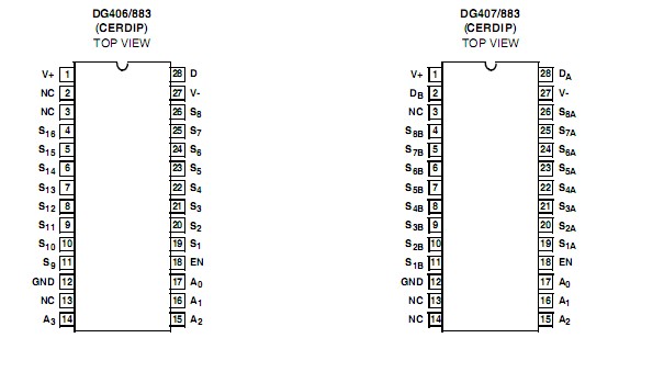 Specifications
V+. . . . . . . . . . . . . . . . . . . . . . . . . . . . . . . . . . . . . . . .. . . . .+44.0V
GND . . . . . . . . . . . . . . . . . . . . . . . . . . . . . . . . . . . . . ... . . . . . . 25V
Digital Inputs, VS, VD (Note 1). . . . . .(V-) -2V to (V+) +2V or 20mA,
Whichever Occurs First
Current (Any Terminal). . . . . . . . . . . . . . . . . .. . . . . . . . . . . . .30mA
Peak Current, S or D . . . . . . . . . . . . . . . . . . . . . . . . . . . . . .100mA
CERDIP Package . . . . . . . . ...................................... . . . . . . . 5512
Maximum Junction Temperature. . . . . . . . . . . . . . . . .. . . . . .150oC
Maximum Storage Temperature Range . . . . . . . . .-65oC to 150oC
DescriptionThe DG406/883 and DG407/883 monolithic CMOS analog multiplexers are drop-in replacements for the popular DG506A/883 and DG507A/883 series devices. They each include an array of sixteen analog switches, a TTL and CMOS compatible digital decode circuit for channel selec- tion, a voltage reference for logic thresholds, and an ENABLE input for device selection when several multiplex-ers are present.
These DG406/883 and DG407/883 feature lower signal ON resistance(<100Ω) and faster transition time (tTRANS <250ns) compared to the DG506A/883 and DG507A/883. Charge injection has been reduced, simplifying sample and hold applications.
The improvements in the DG406 series are made possible by using a high voltage silicon-gate process. An epitaxial layer prevents the latch-up associated with older CMOS technolo-gies. The 44V maximum voltage range permits controlling 30VP-P signals when operating with ±15V power supplies.
The sixteen switches are bilateral, equally matched for AC or bidirectional signals. The ON resistance variation with analog signals is quite low over a ± 5V analog input range

 DG407/883 Data Sheet