Features: ` No Power-Supply Sequencing Required
` Rail-to-Rail Signal Handling
` All Switches Off with Power Off
` All Switches Off when V+ is Off and V- is On
` ±40V Fault Protection with Power Off
` ±36V Fault Protection with ±15V Supplies
` Control Line Fault Protection from V- - 0.3V to V- + 40V
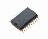
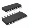
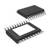
` Pin Compatible with Industry-Standard DG411/DG412/DG413
` 20ns (typ) Fault Response Time
` 35 (max) RON with ±15V Supplies
` ±4.5V to ±20V Dual Supplies
` +9V to +36V Single Supply
` TTL- and CMOS-Compatible Logic Inputs with ±15V or Single +9V to +15V SuppliesApplication·Communication Systems
·Signal Routing
·Test Equipment
·Data Acquisition
·Industrial and Process Control Systems
·Avionics
·Redundant/Backup SystemsPinout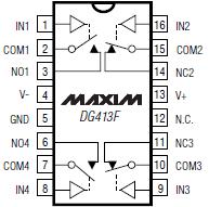
Specifications(Voltages Referenced to GND)
V+...........................................................................-0.3V to +44V
V- ...........................................................................-44V to +0.3V
V+ to V-..................................................................-0.3V to +44V
IN_ ......................................................... (V- - 0.3V) to (V- + 40V)
NO_, NC_ to COM_ (Note1) ................................... -40V to +40V
COM_, NO_, NC_ Voltage with
Power On (Note 1)................................................. -36V to +36V
COM_, NO_, NC_ Voltage with
Power Off (Note 1)................................................. -40V to +40V
Continuous Current (any terminal) ................................ ±30mA
Peak Current COM_, NO_, NC_
(pulsed at 1ms, 10% duty cycle) ...................................±100mA
Continuous Power Dissipation (TA = +70°C)
16-Pin TSSOP (derate 9.4mW/°C above +70°C) ......... 755mW
16-Pin SO (derate 8.7mW/°C above +70°C).................696mW
16-Pin Plastic DIP (derate 10.53mW/°C
above +70°C) ............................................................... 842mW
Operating Temperature Range ....................... -40°C to +85°C
Junction Temperature ................................................... +150°C
Storage Temperature Range ......................... -65°C to +160°C
Lead Temperature (soldering, 10s) ............................... +300°C
Note 1: COM_, NO_, and NC_ pins are fault protected. Signals on COM_, NO_, and NC_ exceeding -36V to +36V may damage the device during power-on conditions. When the power is off, the maximum range is -40V to +40V.
Stresses beyond those listed under "Absolute Maximum Ratings" may cause permanent damage to the device. These are stress ratings only, and functional operation of the device at these or any other conditions beyond those indicated in the operational sections of the specifications is not implied. Exposure to absolute maximum rating conditions for extended periods may affect device reliability.
DescriptionThe DG411F/DG412F/DG413F are quad, single-pole/single- throw (SPST), fault-protected analog switches. They are pin compatible with the industry-standard nonprotected DG411/DG412/DG413. These new switchesDG411F/DG412F/DG413F feature fault-protected inputs and Rail-to-Rail®signalhandling capability. All terminals are protected from overvoltage faults up to ±36V with power on and up to ±40V with power off. During a fault condition, the COM, NO, or NC terminal becomes an open circuit and only microamperes of leakage current flow from the source. On-resistance is 35 (max) and is matched between switches to 1.5 (max) at +25°C.
The DG411F has four normally closed (NC) switches. The DG412F has four normally open (NO) switches. The DG413F has two NC and two NO switches. These CMOS switches operate with dual power supplies ranging from ±4.5V to ±20V or a single supply between +9V and +36V. All digital inputs have +0.8V and +2.4V logic thresholds, ensuring both TTL and CMOS logic compatibility when using ±15V or a single +12V supply.
For supply voltages of ±5V, +5V, and +3V, refer to the MAX4711/MAX4712/MAX4713 data sheet.

 DG413F Data Sheet