Features: ` Operates at NRZ data rates up to 50 Mbits/sec (equivalent 2/3 (1,7) code data rate)
` Operates with a single a 5V power supply
` Multiple power down modes available with dedicated SLEEP and IDLE/SERVO power down pins
` Sleep mode included where ICC e 2 mA maximum
` Directly addresses zoned data recording requirements
-- Integrated channel filter with selectable equalization and bandwidth eliminates multiple external filter elements
-- Fully integrated frequency synthesizer on-chip to provide write clock and center frequency for the synchronizer
` Selectable delay impedance switch (clamp) at pulse detector input for rapid recovery from the write mode
` Pattern insensitive fast AGC for rapid head switch settling and embedded servo normalization
` Built-in AGC hold for embedded servo
` Two AGC control voltage pins providedÐone for servo field and one for data field
` Four gated detectors for quadrature embedded servo information
`Two servo difference amplifiers on-chip
` Reference voltage input pin provided for the servo difference amplifiers
` Two selectable hysteresis control pins provided-one for servo field and one for data field
` Data field hysteresis level is control register selectable in eight steps
` Logic polarity for write gate assertion is control register selectable
` Capability provided for different channel filter bandwidths for servo and data fieldsÐchange on the fly with no settling issues
` Selectable qualification channel delay
` Dual gain synchronizer requiring no external or internal center frequency setting components, external adjustments, or precision components
` Digitally controlled synchronizer window strobing
` Zero-phase-start synchronizer lock acquisition
` Two port synchronizer PLL filtering
` Frequency lock option for 2T or 3T synchronization field (preamble)
` TTL compatible inputs and outputs
` Chip configurable through serial port interfacePinout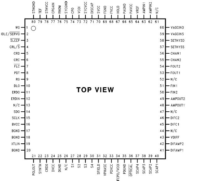 SpecificationsSupply Voltage 7V
TTL Input Maximum Voltage 7V
Maximum Output Voltage 7V
Maximum Input Current (Analog Pins) 2 mA
(or as specified on per-pin basis)
ESD Susceptibility 1500V
(Note 1)DescriptionThe DP84910 integrates most functions of the hard disk read channel electronics onto a single 5V chip. DP84910 incorporates a pulse/servo detector, a programmable integrated channel filter, a data synchronizer, a frequency synthesizer, and a serial port interface. The chip receives data from a read preamplifier, filters and peak detects the read pulses for both data and embedded servo information and resynchronizes the data with the system clock.
The DP84910 is available in two versions, DP84910VHG-36 and DP84910VHG-50. The DP84910VHG-36 is specified to operate over a data rate range of 7.5 Mbits/sec to 36 Mbits/sec.
The other version, DP84910VHG-50, will operate over a data rate range of 13.7 Mbits/sec to 50 Mbits/ sec. DP84910 is specifically designed to address zoned data rate applications. A channel filter with control register selectable cutoff frequency and equalization is provided onchip. This eliminates the need for multiple external channel filters and allows for greater flexibility in the selection of zone frequencies. The frequency synthesizer provides center frequency information for the data synchronizer and a variable frequency write clock. There is no need for any offchip frequency setting components or DACs. A four-bank control register is included to control zoning operations and configure general chip functions. At VCC power-up DP84910 self-configures by presetting all bits in the control register to predetermined operating setup conditions. Independent power down control for all of the major blocks within the chip is provided via three bits in the control register (SYNC_PWR_DN, STH_PWR_DN and PD_PWR_DN) to manage power consumption. In addition, two pins (SLEEP and IDLE/SERVO) are available to control power management. The sleep mode pin (SLEEP) powers down all circuitry on the chip including the control register. In this mode the maximum power supply current is 2 mA; the control register data must be reentered when exiting this mode. The idle/servo mode pin (IDLE/SERVO) toggles the device between the idle and servo modes. In the idle mode, only the control register and pulse detector biasing circuitry necessary for a quick recovery are active. In the servo mode, the pulse detector DP84910 portions needed for servo detection are active as well as the control register. Less than 15 ms is required for the pulse detector to recover from the idle condition. The control register data is not lost when this pin is toggled. The pin can be rapidly toggled (k15 ms) to achieve average power consumption savings and will keep the read/write head on track. Seventeen power and ground pins are provided to isolate major functional blocks and allow for independent supply voltage filtering, thus enhancing noise immunity.
The pulse detector section of the DP84910 detects the peaks of the analog pulses from the read preamplifier and converts them to digital pulses whose leading edges represent the time position of the analog pulses' peaks. In order to not interpret noise on the baseline as input data, hysteresis is included. The hysteresis level for a data field is set at the SETHYSD pin while the hysteresis level for a servo field is set at the SETHYSS pin. A third pin (SFIELD) is used to select between these two levels of hysteresis. This allows for the setting of different hysteresis levels for these two fields. The data field hysteresis level is also selectable in 8 steps through bits in the control register (HYS_VTH0±HYS_ VTH2) with the level set at the SETHYSD pin as the nominal value. The pulse detector section of the DP84910 includes an automatic gain control (AGC) circuit which normalizes the analog data signal to a constant amplitude. The response of the AGC is partially controlled by one of the device's pins (VAGCIN). Two VAGCIN pins (VAGCIND, VAGCINS) are provided so that different capacitor values can be selected to provide different AGC time constants for data and servo field information. The switching between these pins/capacitors is controlled by the SFIELD pin. The SERVO control register bit can enable (or disable) the SFIELD pin's ability to control the amount of equalization provided to the on-chip channel filter. When enabled, the state of the SFIELD pin selects between two groups of control register bits (EQ0, EQ1, EQ2 and SERVO_EQ0, SERVO_EQ1, SERVO_EQ2) which can separately determine the amount of equalization provided. This feature allows for an adjustment of the channel filter bandwidth in a servo field. Thus the channel filter can have different bandwidths in a servo field and a data field. The pulse detector section of the DP84910 has a delayed, low impedance switch at the gain controlled amplifier inputs (AMPIN1, AMPIN2) which allows for rapid recovery from the write mode. The amount of delay (either 1.7 ms or 3.4 ms) coming out of the low impedance mode is selectable through a bit in the control register (SLOW). A pattern insensitive, fast responding AGC circuit (with HOLD function) allows rapid head switch settling and embedded servo normalization. Selectable delay (in four steps) in the qualification channel, along with a ``view internal signals'' mode, allow the timing and qualification channels to be optimally aligned. Four gated servo detectors are incorporated for recovery of quadrature embedded servo information. The four peak detected values are available at the SERVO CAPACITOR outputs (SCAP1±4). Two servo difference amplifiers are provided. Each difference amplifier output (DIFFAMP1/2) provides the difference between two of the servo peak detectors, centered about an external reference voltage (VDIFF). The channel filter section is a seven-pole 0.05 degree error, equal ripple filter. It utilizes the Kost pulse slimming technique similar to that which is employed on the DP8491/92 integrated read channel devices. The amount of pulse slimming is control register selectable in 8 steps up to a maximum of 9 dB measured from the base frequency. The bandwidth of the filter is derived from the XTLIN frequency; from this point, the b3 dB frequency is selectable via 7 bits in the control register (FILT_3 dB_0±FILT_3 dB_6). The data synchronizer section incorporates zero-phasestart (ZPS) and digitally controlled window strobe functions.
The voltage controlled oscillator (VCO) is fully integrated, requiring no external components, and provides a wide dynamic range necessary for zoned data rate applications. Data windowing is based on precise VCO duty cycle symmetry (in contrast to delay line based centering). An internal silicon delay line, used to establish the phase detector DP84910 retrace angle, automatically tracks zoned data recording data rate changes. The charge pump output (CPO) and voltage controlled oscillator input (VCOI) are provided as separate pins, allowing ample design flexibility in the external loop filter. Frequency lock may be employed within the synchronization field.
Charge pump (phase detector) gain may be selected to remain constant or to vary either by a factor of two or four as instructed via the charge pump gain pin (CPGAIN) and a bit in the control register (CPRATIO). The frequency synthesizer section, capable of producing a large number of frequencies from a single external reference source, generates the write clock and reference frequency for the synchronizer. This section includes a phase locked loop (PLL) with selectable dividers at the input port and in its feedback loop. The values of the DP84910 for the dividers are controlled by two control words within the control register.
The user has full control over both the input (five bit word, PDATA6±PDATA10) and feedback (six bit word, PDATA0± PDATA5) divider selection. The feedback divider has an extra bit when compared to previous NSC integrated read channel circuits to improve the resolution of frequency setting. All blocks within the synthesizer, except the RC loop filter, are fully integrated. The loop filter resides external to the chip giving the user full control over the phase locked loop's dynamics.
DP84910 is available in an 80-pin 12 mm x 12 mm PQFP package and operates off of a single a5V supply.

 DP84910 Data Sheet