Features: Fast propagation delay (3ns typ)
9-BIT BTL Latched Transceiver
Driver incorporates edge triggered latches
Receiver incorporates transparent latches
Meets IEEE 1194.1 Standard on Backplane TransceiverLogic (BTL)
Supports Live Insertion
Glitch free Power-up/down protection
Typically less than 5 pF Bus-port capacitance
Low Bus-port voltage swing (typically 1V) at 80 mAPinout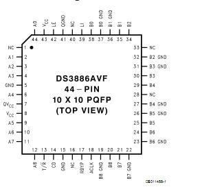 SpecificationsIf Military/Aerospace specified devices are required,
please contact the National Semiconductor Sales Office/
Distributors for availability and specifications.
Supply Voltage ......................................................6.5V
Control Input Voltage...................................... ..... 6.5V
Driver Input and Receiver
Output ..................................................................5.5V
Receiver Input Current ....................................±15 mA
Bus Termination Voltage .......................................2.4V
Power Dissipation at........................................... . 25˚C
PLCC (V44A) ...................................................... ..2.5W
PQFP (VF44B) ........................................................1.3W
Derate PLCC Package (V44A) .........................20 mW/˚C
Derate PQFP Package
(VF44B) .......................................................11.1 mW/˚C
Storage Temperature Range ...............−65˚C to +150˚C
Lead Temperature (Soldering, 4sec.)................. . 260˚CDescriptionThe DS3886A is a higher speed, lower power, pin compat-ible version of the DS3886.
The DS3886A is one in a series of transceivers designedspecifically for the implementation of high performance Fu-turebus+ and proprietary bus interfaces. The DS3886A is aBTL 9-Bit Latching Data Transceiver designed to conform toIEEE 1194.1 (Backplane Transceiver Logic-BTL) as speci-
fied in the IEEE 896.2 Futurebus+ specification. TheDS3886A incorporates an edge-triggered latch in the driverpath which can be bypassed during fall-through mode of op-eration and a transparent latch in the receiver path. Utiliza-tion of the DS3886A simplifies the implementation of bytewide address/data with parity lines and also may be used forthe Futurebus+ status, tag and command lines.
The DS3886A driver output configuration is an NPN opencollector which allows Wired-OR connection on the bus.Each driver output incorporates a Schottky diode in serieswith it's collector to isolate the transistor output capacitancefrom the bus, thus reducing the bus loading in the inactivestate. The combined output capacitance of the driver outputand receiver input is less than 5 pF. The driver also has high
sink current capability to comply with the bus loading re-quirements defined within IEEE 1194.1 BTL specification.
Backplane Transceiver Logic (BTL) is a signaling standardthat was invented and first introduced by National Semicon-ductor, then developed by the IEEE to enhance the perfor-mance of backplane buses. BTL compatible transceiversfeature low output capacitance drivers to minimize bus load-ing, a 1V nominal signal swing for reduced power consump-tion and receivers with precision thresholds for maximumnoise immunity. The BTL standard eliminates settling timedelays that severely limit TTL bus performance, and thusprovide significantly higher bus transfer rates. The back-plane bus is intended to be operated with termination resis-tors (selected to match the bus impedance) connected to2.1V at both ends. The low voltage is typically 1V.Separate ground pins are provided for each BTL output tominimize induced ground noise during simultaneous switch-ing.
The unique driver circuitry meets the maximum slew rate of0.5 V/ns which allows controlled rise and fall times to reducenoise coupling to adjacent lines.The transceiver's high impedance control and driver inputsare fully TTL compatible.The receiver is a high speed comparator that utilizes a Band-gap reference for precision threshold control, allowing maxi-mum noise immunity to the BTL 1V signaling level. Separate
QVCC and QGND pins are provided to minimize the effectsof high current switching noise. The output is TRI-STATE®and fully TTL compatible.The DS3886A supports live insertion as defined in IEEE896.2 through the LI (Live Insertion) pin. To implement liveinsertion the LI pin should be connected to the live insertionpower connector. If this function is not supported, the LI pinmust be tied to the VCC pin. The DS3886A also providesglitch free power up/down protection during power sequenc-ng.
The DS3886A has two types of power connections in addi-ion to the LI pin. They are the Logic VCC (VCC) and the QuieVCC (QVCC). There are two Logic VCC pins on the DS3886Ahat provide the supply voltage for the logic and control cir-cuitry. Multiple connections are provided to reduce the ef-ects of package inductance and thereby minimize switchingnoise. As these pins are common to the VCC bus internal to
he device, a voltage delta should never exist between thesepins and the voltage difference between V CC and QVCCshould never exceed ±0.5V because of ESD circuitry.When CD (Chip Disable) is high, An is in high impedancestate and Bn is high. To transmit data (An to Bn) the T/R sig-
nal is high.When RBYP is high, the positive edge triggered flip-flop is inhe transparent mode. When RBYP is low, the positive edgeof the ACLK signal clocks the data.n addition, the ESD circuitry between the VCC pins and alother pins except for BTL I/O's and LI pins requires that anyvoltage on these pins should not exceed the voltage on VCC+0.5V.
There are three different types of ground pins on theDS3886A; the logic ground (GND), BTL grounds(B0GNDB8GND) and the Bandgap reference ground(QGND). All of these ground reference pins are isolatedwithin the chip to minimize the effects of high current switch-ing transients. For optimum performance the QGND shouldbe returned to the connector through a quiet channel thatdoes not carry transient switching current. The GND andB0GNDB8GND should be connected to the nearest back-plane ground pin with the shortest possible path.Since many different grounding schemes could be imple-
mented and ESD circuitry exists on the DS3886A, it is impor-tant to note that any voltage difference between ground pins,QGND, GND or B0GNDB8GND should not exceed ±0.5Vincluding power up/down sequencing.The DS3886A is offered in 44-pin PLCC, and 44-pin PQFPhigh density package styles.

 DS3886A Data Sheet