Features: ·>155.5 Mbps (77.7 MHz) switching rates
·Accepts small swing (350 mV) differential signal levels
·Ultra low power dissipation
·600 ps maximum differential skew (5V, 25°C)
·6.0 ns maximum propagation delay
·Industrial operating temperature range
·Military operating temperature range option
·Available in surface mount packaging (SOIC) and (LCC)
·Pin compatible with DS26C32A, MB570 (PECL) and 41LF (PECL)
·Supports OPEN, short and terminated input fail-safe
·Compatible with IEEE 1596.3 SCI LVDS standard
·Conforms to ANSI/TIA/EIA-644 LVDS standard
·Available to Standard Microcircuit Drawing (SMD) 5962-95834Pinout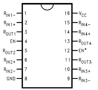 SpecificationsSupply Voltage (VCC) −0.3V to +6V
Input Voltage (RIN+, RIN−)−0.3V to (VCC +0.3V)
Enable Input Voltage (EN, EN*)−0.3V to (VCC +0.3V)
Output Voltage (ROUT) −0.3V to (VCC +0.3V)
Maximum Package Power Dissipation @ +25°C
M Package 1025 mW
E Package1830 mW
Derate M Package 8.2 mW/°C above +25°C
Derate E Package 12.2 mW/°C above +25°C
Storage Temperature Range −65°C to +150°C
Lead Temperature Range Soldering (4 sec.)+260°C
Maximum Junction Temperature (DS90C032T)+150°C
Maximum Junction Temperature (DS90C032E)+175°C
ESD Rating (Note 7)
(HBM, 1.5 kΩ, 100 pF) 3,500V
(EIAJ, 0 Ω, 200 pF) 250V
| PHY Type |
Receiver |
| Family |
LVDS |
| Channels |
4 Channels |
| Max Data Rate |
155 Mbps |
| Input Compatibility |
LVDS |
| Output Compatibility |
TTL |
| Power Consumption_ |
18 mW |
| SupplyVoltage |
5 Volt |
| JTAG1149.1 |
No |
| Temperature Min |
-40 deg C |
| Temperature Max |
85 deg C |
| Function |
Receiver |
| View Using Catalog |
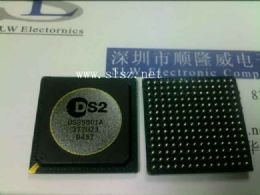
DescriptionTheDS90C032 is a quad CMOS differential line receiver designed for applications requiring ultra low power dissipation and high data rates. The device is designed to support data rates in excess of 155.5 Mbps (77.7 MHz) utilizing Low Voltage Differential Signaling (LVDS) technology.
TheDS90C032 accepts low voltage (350 mV) differential input signals and translates them to CMOS (TTL compatible) output levels. The receiver supports a TRI-STATE® function that may be used to multiplex outputs. The receiver also supports OPEN, shorted and terminated (100Ω) input Failsafe with the addition of external failsafe biasing. Receiver output will be HIGH for both Failsafe conditions.
TheDS90C032 and companion line driver (DS90C031) provide a new alternative to high power psuedo-ECL devices for high speed point-to-point interface applications.
The DS90C032 is a quad CMOS differential line receiver designed for applications requiring ultra low power dissipation and high data rates. The device is designed to support data rates in excess of 155.5 Mbps (77.7 MHz) utilizing Low Voltage Differential Signaling (LVDS) technology.
The DS90C032 accepts low voltage (350 mV) differential input signals and translates them to CMOS (TTL compatible) output levels. The receiver supports a TRI-STATE function that may be used to multiplex outputs. The receiver also supports OPEN, shorted and terminated (100) input Failsafe with the addition of external failsafe biasing. Receiver output will be HIGH for both Failsafe conditions.
The DS90C032 and companion line driver (DS90C031) provide a new alternative to high power psuedo-ECL devices for high speed point-to-point interface applications.
Reliability Metrics
| Part Number |
Process |
EFR Reject |
EFR Sample Size |
PPM |
LTA Rejects |
LTA Device Hours |
FITS |
MTTF (Hours) |
| DS90C032 MD8 |
CS080 |
0 |
29095 |
0 |
0 |
2720500 |
2 |
771949303 |
| DS90C032 MDR |
CS080 |
0 |
29095 |
0 |
0 |
2720500 |
2 |
771949303 |
| DS90C032TM |
CS080 |
0 |
29095 |
0 |
0 |
2720500 |
2 |
771949303 |
| DS90C032TMX |
CS080 |
0 |
29095 |
0 |
0 |
2720500 |
2 |
771949303 |
| DS90C032W-MLS |
CS080 |
0 |
29095 |
0 |
0 |
2720500 |
2 |
771949303 |
| DS90C032W-QMLV |
CS080 |
0 |
29095 |
0 |
0 |
2720500 |
2 |
771949303 |
| DS90C032WG-QMLV |
CS080 |
0 |
29095 |
0 |
0 |
2720500 |
2 |
771949303 |
| DS90C032WGLQMLV |
CS080 |
0 |
29095 |
0 |
0 |
2720500 |
2 |
771949303 |
| DS90C032WLQMLV |
CS080 |
0 |
29095 |
0 |
0 |
2720500 |
2 |
771949303 |
Note: The Early Failure Rates (EFR) were calculated as point estimate PPM based on rejects and sample size for EFR. The Long Term Failure Rates were calculated at 60% confidence using the Arrhenius equation at 0.7eV activation energy and derating the assumed stress temperature of 150°C to an application temperature of 55°C.For more information on Reliability Metrics, please click here.
Application Notes
| Title |
Size in Kbytes |
Date |
|
| AN-1110: Application Note 1110 LVDS Quad Dynamic I CC vs Frequency |
159 Kbytes |
4-Oct-04 |
Download |
| AN-971: Application Note 971 An Overview of LVDS Technology |
168 Kbytes |
5-Oct-98 |
Download |
AN-971 (Japanese): Application Note 971 An Overview of LVDS Technology
640){this.height=this.height*640/this.width;this.width=640;}' border="0" alt=" Connection Diagram"> |
168 Kbytes |
|
|
| AN-1040: Application Note 1040 LVDS Performance: Bit Error Rate (BER) Testing Test Report [num]2 |
43 Kbytes |
4-Oct-04 |
Download |
If you have trouble printing or viewing PDF file(s), see Printing Problems.
|
More Application Notes
| Title |
Size in Kbytes |
Date |
|
| AN-1088: Application Note 1088 LVDS Signal Quality: Cable Drive Measurements using Eye Patterns Test Report #3 |
130 Kbytes |
4-Oct-04 |
Download |
| AN-1934: Application Note 1934 Failsafe Options for LVDS Receivers |
122 Kbytes |
20-Jan-09 |
Download |
| AN-977: Application Note 977 LVDS Signal Quality: Jitter Measurements Using Eye Patterns Test Report #1 |
63 Kbytes |
5-Oct-98 |
Download |
AN-977 (Japanese): Application Note 977 LVDS Signal Quality: Jitter Measurements Using Eye Patterns Test Report #1
640){this.height=this.height*640/this.width;this.width=640;}' border="0" alt=" Connection Diagram"> |
104 Kbytes |
|
|
If you have trouble printing or viewing PDF file(s), see Printing Problems.
|

 DS90C032 Data Sheet