DS90LV018A

Features: >400 Mbps (200 MHz) switching rates50 ps differential skew (typical)2.5 ns maximum propagation delay3.3V power supply designFlow-through pinoutPower down high impedance on LVDS inputsLow Power design (18mW @ 3.3V static)Interoperable with existing 5V LVDS networksAccepts small swing (...

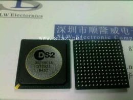
product image

DS90LV018A Picture
SeekIC No. : 004329390 Detail

DS90LV018A: Features: >400 Mbps (200 MHz) switching rates50 ps differential skew (typical)2.5 ns maximum propagation delay3.3V power supply designFlow-through pinoutPower down high impedance on LVDS inputsLo...

floor Price/Ceiling Price

Part Number:
DS90LV018A
Supply Ability:
5000

Price Break

  • Qty
  • 1~5000
  • Unit Price
  • Negotiable
  • Processing time
  • 15 Days
Total Cost: $ 0.00

SeekIC Buyer Protection PLUS - newly updated for 2013!

  • Escrow Protection.
  • Guaranteed refunds.
  • Secure payments.
  • Learn more >>

Month Sales

268 Transactions

Rating

evaluate  (4.8 stars)

Upload time: 2024/4/26

Payment Methods

All payment methods are secure and covered by SeekIC Buyer Protection PLUS.

Notice: When you place an order, your payment is made to SeekIC and not to your seller. SeekIC only pays the seller after confirming you have received your order. We will also never share your payment details with your seller.
Product Details

Description


Features:

>400 Mbps (200 MHz) switching rates
50 ps differential skew (typical)
2.5 ns maximum propagation delay
3.3V power supply design
Flow-through pinout
Power down high impedance on LVDS inputs
Low Power design (18mW @ 3.3V static)
Interoperable with existing 5V LVDS networks
Accepts small swing (350 mV typical) differential signal levels
Supports open, short and terminated input fail-safe
Conforms to ANSI/TIA/EIA-644 Standard
Industrial temperature operating range (−40°C to +85°C)
Available in SOIC package


Application

General application guidelines and hints for LVDS drivers and receivers may be found in the following application notes: LVDS Owner's Manual (lit #550062-001), AN808, AN1035, AN977, AN971, AN916, AN805, AN903.

LVDS drivers and receivers are intended to be primarily used in an uncomplicated point-to-point configuration as is shown in Figure 3. This configuration provides a clean signaling environment for the fast edge rates of the drivers. The receiver is connected to the driver through a balanced media which may be a standard twisted pair cable, a parallel pair cable, or simply PCB traces. Typically the characteristic impedance of the media is in the range of 100W. A termination resistor of 100W should be selected to match the media, and is located
as close to the receiver input pins as possible. The termination resistor converts the driver output (current mode) into a voltage that is detected by the receiver. Other configurations are possible such as a multi-receiver configuration, but the effects of a mid-stream connector(s), cable stub(s), and other impedance discontinuities as well as ground shifting, noise margin limits, and total termination loading must be taken into account.

The DS90LV018A differential line receiver is capable of detecting signals as low as 100 mV, over a ±1V common-mode range centered around +1.2V. This is related to the driver offset voltage which is typically +1.2V. The driven signal is centered around this voltage and may shift ±1V around this center point. The ±1V shifting may be the result of a ground potential difference between the driver's ground reference and the receiver's ground reference, the common-mode effects of coupled noise, or a combination of the two. The AC parameters of both receiver input pins are optimized for a recommended operating input voltage range of 0V to +2.4V (measured from each pin to ground). The device will still operate for receivers input voltages up to VCC, but exceeding VCC will turn on the ESD protection circuitry which will clamp the bus voltages.


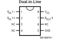
Pinout

  Connection Diagram


Specifications

PHY Type Receiver
Family LVDS
Channels 1 Channels
Max Data Rate 400 Mbps
Input Compatibility LVDS
Output Compatibility LVTTL
Power Consumption_ 18 mW
Special Features >7kV ESD
SupplyVoltage 3.3 Volt
JTAG1149.1 No
Temperature Min -40 deg C
Temperature Max 85 deg C
Function Receiver
View Using Catalog


Description

The DS90LV018A is a single CMOS differential line receiver designed for applications requiring ultra low power dissipation, low noise and high data rates. The device is designed to support data rates in excess of 400 Mbps (200 MHz) utilizing Low Voltage Differential Signaling (LVDS) technology.

The DS90LV018A accepts low voltage (350 mV typical) differential input signals and translates them to 3V CMOS output levels. The receiver also supports open, shorted and terminated (100) input fail-safe. The receiver output will be HIGH for all fail-safe conditions. The DS90LV018A has a flow-through design for easy PCB layout.

The DS90LV018A and companion LVDS line driver provide a new alternative to high power PECL/ECL devices for high speed point-to-point interface applications.

Reliability Metrics


Part Number Process EFR Reject EFR Sample Size PPM LTA Rejects LTA Device Hours FITS MTTF (Hours)
DS90LV018ATM .35 0 18700 0 0 1290000 3 366041022
DS90LV018ATMX .35 0 18700 0 0 1290000 3 366041022

Note: The Early Failure Rates (EFR) were calculated as point estimate PPM based on rejects and sample size for EFR. The Long Term Failure Rates were calculated at 60% confidence using the Arrhenius equation at 0.7eV activation energy and derating the assumed stress temperature of 150°C to an application temperature of 55°C.

For more information on Reliability Metrics, please click here.


Customers Who Bought This Item Also Bought

Margin,quality,low-cost products with low minimum orders. Secure your online payments with SeekIC Buyer Protection.
Undefined Category
Audio Products
Test Equipment
Cable Assemblies
Industrial Controls, Meters
Batteries, Chargers, Holders
View more