DS90LV019

Features: ·LVDS Signaling·3.3V or 5.0V operation·Low power CMOS design·Balanced Output Impedance·Glitch free power up/down (Driver disabled)·High Signaling Rate Capacity (above 100 Mbps)·Ultra Low Power Dissipation·±1V Common-Mode Range·±100 mV Receiver Sensitivity·Product offered in SOIC and TSSO...

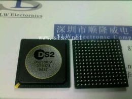
product image

DS90LV019 Picture
SeekIC No. : 004329391 Detail

DS90LV019: Features: ·LVDS Signaling·3.3V or 5.0V operation·Low power CMOS design·Balanced Output Impedance·Glitch free power up/down (Driver disabled)·High Signaling Rate Capacity (above 100 Mbps)·Ultra Low P...

floor Price/Ceiling Price

Part Number:
DS90LV019
Supply Ability:
5000

Price Break

  • Qty
  • 1~5000
  • Unit Price
  • Negotiable
  • Processing time
  • 15 Days
Total Cost: $ 0.00

SeekIC Buyer Protection PLUS - newly updated for 2013!

  • Escrow Protection.
  • Guaranteed refunds.
  • Secure payments.
  • Learn more >>

Month Sales

268 Transactions

Rating

evaluate  (4.8 stars)

Upload time: 2024/4/26

Payment Methods

All payment methods are secure and covered by SeekIC Buyer Protection PLUS.

Notice: When you place an order, your payment is made to SeekIC and not to your seller. SeekIC only pays the seller after confirming you have received your order. We will also never share your payment details with your seller.
Product Details

Description


Features:

·LVDS Signaling
·3.3V or 5.0V operation
·Low power CMOS design
·Balanced Output Impedance
·Glitch free power up/down (Driver disabled)
·High Signaling Rate Capacity (above 100 Mbps)
·Ultra Low Power Dissipation
·±1V Common-Mode Range
·±100 mV Receiver Sensitivity
·Product offered in SOIC and TSSOP packages
·Flow-Through Pin Out
·Industrial Temperature Range Operation


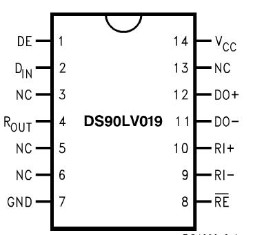
Pinout


Specifications

Supply Voltage VCC 6.0V
Enable Input Voltage (DE, RE) −0.3V to (VCC +0.3V)
Driver Input Voltage (DIN) −0.3V to (VCC + 0.3V)
Receiver Output Voltage (ROUT) −0.3V to (VCC + 0.3V)
Driver Output Voltage (DO±) −0.3V to +3.9V
Receiver Input Voltage (RI±) −0.3V to (VCC + 0.3V)
Driver Short Circuit Current Continuous
ESD (Note 4)
(HBM, 1.5 kW, 100 pF) > 2.0 kV
(EIAJ, 0 W, 200 pF) > 200 V
Maximum Package Power Dissipation at25°C
SOIC 960 mW
Derate SOIC Package 7.7mW/°C
TSSOP 790 mW
Derate TSSOP Package 6.3mW/°C
Storage Temperature Range −65°C to +150°C
Lead Temperature (Soldering, 4 sec.) 260°C


Description

The DS90LV019 is a Driver/Receiver designed specifically for the high speed low power point-to-point interconnect applications.

The DS90LV019 device operates from a single 3.3V or 5.0V power supply and includes one differential line driver and one receiver. The DS90LV019 features an independent driver and receiver with TTL/CMOS compatibility (DIN and ROUT). The logic interface provides maximum flexibility as 4 separate lines are provided (DIN, DE, RE, and ROUT). The device also features a flow-through pin out which allows easy PCB routing for short stubs between its pins and the connector. The driver has 3.5 mA output loop current.

The DS90LV019 driver translates between TTL levels (single-ended) to Low Voltage Differential Signaling levels. This allows for high speed operation, while consuming minimal power with reduced EMI. In addition, the differential signaling provides common-mode noise rejection.

The DS90LV019 receiver threshold is ±100 mV over a ±1V commonmode range and translates the low swing differential levels to standard (TTL/CMOS) levels.


Customers Who Bought This Item Also Bought

Margin,quality,low-cost products with low minimum orders. Secure your online payments with SeekIC Buyer Protection.
Circuit Protection
Power Supplies - Board Mount
Semiconductor Modules
RF and RFID
Prototyping Products
DE1
Transformers
View more