DS90LV049H

Features: ·High Temperature +125°C Operating Range· Up to 400 Mbps switching rates· Flow-through pinout simplifies PCB layout· 50 ps typical driver channel-to-channel skew· 50 ps typical receiver channel-to-channel skew· 3.3 V single power supply design· TRI-STATE output control· Internal fail-saf...

product image

DS90LV049H Picture
SeekIC No. : 004329402 Detail

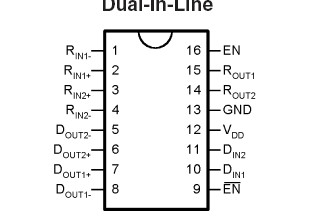
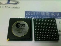
DS90LV049H: Features: ·High Temperature +125°C Operating Range· Up to 400 Mbps switching rates· Flow-through pinout simplifies PCB layout· 50 ps typical driver channel-to-channel skew· 50 ps typical receiver ch...

floor Price/Ceiling Price

Part Number:
DS90LV049H
Supply Ability:
5000

Price Break

  • Qty
  • 1~5000
  • Unit Price
  • Negotiable
  • Processing time
  • 15 Days
Total Cost: $ 0.00

SeekIC Buyer Protection PLUS - newly updated for 2013!

  • Escrow Protection.
  • Guaranteed refunds.
  • Secure payments.
  • Learn more >>

Month Sales

268 Transactions

Rating

evaluate  (4.8 stars)

Upload time: 2024/4/26

Payment Methods

All payment methods are secure and covered by SeekIC Buyer Protection PLUS.

Notice: When you place an order, your payment is made to SeekIC and not to your seller. SeekIC only pays the seller after confirming you have received your order. We will also never share your payment details with your seller.
Product Details

Description


Features:

·High Temperature +125°C Operating Range
· Up to 400 Mbps switching rates
· Flow-through pinout simplifies PCB layout
· 50 ps typical driver channel-to-channel skew
· 50 ps typical receiver channel-to-channel skew
· 3.3 V single power supply design
· TRI-STATE output control
· Internal fail-safe biasing of receiver inputs
·Low power dissipation (70 mW at 3.3 V static)
·High impedance on LVDS outputs on power down
· Conforms to TIA/EIA-644-A LVDS Standard
·Available in low profile 16 pin TSSOP package


Pinout

  Connection Diagram


Specifications

Supply Voltage (VDD) ................................................................−0.3 V to +4 V
LVCMOS Input Voltage (DIN) .......................................−0.3 V to (VDD + 0.3 V)
LVDS Input Voltage (RIN+, RIN-) ............................................−0.3 V to +3.9 V
Enable Input Voltage (EN, EN) .....................................−0.3 V to (VDD + 0.3 V)
LVCMOS Output Voltage (ROUT) ..................................−0.3 V to (VDD + 0.3 V)
LVDS Output Voltage
(DOUT+, DOUT-) .....................................................................−0.3 V to +3.9 V
LVCMOS Output Short Circuit
Current (ROUT) .....................................................................................100 mA
LVDS Output Short Circuit
Current (DOUT+, DOUT−) ........................................................................24mA
LVDS Output Short Circuit
Current Duration(DOUT+, DOUT−) .................................................Continuous
Storage Temperature Range .............................................−65°C to +150°C
Lead Temperature Range
Soldering (4 sec.)............................................................................... +260°C
Maximum Junction Temperature .........................................................+150°C
Maximum Package Power Dissipation @ +25°C
MTC Package ......................................................................................866 mW
Derate MTC Package .............................................6.9 mW/°C above +25°C
ESD Rating
(HBM, 1.5 kΩ, 100 pF).......................................................................... 7 kV
(MM, 0 Ω, 200 pF) .............................................................................. 250 V


Description

The DS90LV049H is a dual CMOS flow-through differential line driver-receiver pair designed for applications requiring ultra low power dissipation, exceptional noise immunity, and high data throughput. The device is designed to support data rates in excess of 400 Mbps utilizing Low Voltage Differential Signaling (LVDS) technology.

The DS90LV049H drivers accept LVTTL/LVCMOS signals and translate them to LVDS signals. The receivers accept LVDS signals and translate them to 3 V CMOS signals. The LVDS input buffers have internal failsafe biasing that places the outputs to a known H (high) state for floating receiver inputs. In addition, the DS90LV049H supports a TRI-STATE function for a low idle power state when the device is not in use.

The DS90LV049H EN and EN inputs are ANDed together and control the TRI-STATE outputs. The enables are common to all four gates.


Customers Who Bought This Item Also Bought

Margin,quality,low-cost products with low minimum orders. Secure your online payments with SeekIC Buyer Protection.
Resistors
Discrete Semiconductor Products
Hardware, Fasteners, Accessories
Line Protection, Backups
View more