DS90LV110T

Features: `Low jitter 800 Mbps fully differential data path`145 ps (typ) of pk-pk jitter with PRBS = 223−1 data pattern at 800 Mbps`Single +3.3 V Supply`Less than 413 mW (typ) total power dissipation`Balanced output impedance`Output channel-to-channel skew is 35ps (typ)`Differential output v...

product image

DS90LV110T Picture
SeekIC No. : 004329405 Detail

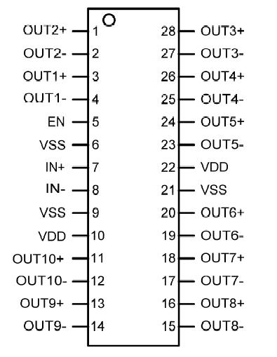
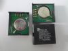
DS90LV110T: Features: `Low jitter 800 Mbps fully differential data path`145 ps (typ) of pk-pk jitter with PRBS = 223−1 data pattern at 800 Mbps`Single +3.3 V Supply`Less than 413 mW (typ) total power diss...

floor Price/Ceiling Price

Part Number:
DS90LV110T
Supply Ability:
5000

Price Break

  • Qty
  • 1~5000
  • Unit Price
  • Negotiable
  • Processing time
  • 15 Days
Total Cost: $ 0.00

SeekIC Buyer Protection PLUS - newly updated for 2013!

  • Escrow Protection.
  • Guaranteed refunds.
  • Secure payments.
  • Learn more >>

Month Sales

268 Transactions

Rating

evaluate  (4.8 stars)

Upload time: 2024/4/26

Payment Methods

All payment methods are secure and covered by SeekIC Buyer Protection PLUS.

Notice: When you place an order, your payment is made to SeekIC and not to your seller. SeekIC only pays the seller after confirming you have received your order. We will also never share your payment details with your seller.
Product Details

Description


Features:

`Low jitter 800 Mbps fully differential data path
`145 ps (typ) of pk-pk jitter with PRBS = 223−1 data pattern at 800 Mbps
`Single +3.3 V Supply
`Less than 413 mW (typ) total power dissipation
`Balanced output impedance
`Output channel-to-channel skew is 35ps (typ)
`Differential output voltage (VOD) is 320mV (typ) with 100 termination load.
`LVDS receiver inputs accept LVPECL signals
`Fast propagation delay of 2.8 ns (typ)
`Receiver input threshold < ±100 mV
`28 lead TSSOP package
`Conforms to ANSI/TIA/EIA-644 LVDS standard


Pinout

  Connection Diagram


Specifications

Supply Voltage (VDD-VSS) −0.3V to +4V
LVCMOS/LVTTL Input Voltage (EN) −0.3V to (VCC + 0.3V)
LVDS Receiver Input Voltage (IN+, IN−) −0.3V to +4V
LVDS Driver Output Voltage (OUT+, OUT−)−0.3V to +4V
Junction Temperature+150°C
Storage Temperature Range−65°C to +150°C
Lead Temperature (Soldering, 4 sec.)+260°C
Maximum Package Power Dissipation at 25°C
28L TSSOP1.209 W
Package Derating 28L TSSOP 9.67 mW/°C above +25°C
JA 28L TSSOP 103.4 °C/Watt
ESD Rating:
(HBM, 1.5kW, 100pF) > 4 kV
(EIAJ, 0W, 200pF)> 250 V


Temperature Min -40 deg C
Temperature Max 85 deg C
SupplyVoltage 3.3 Volt
JTAG1149.1 No
Function 1:n Repeater
View Using Catalog


Description

DS90LV110 is a 1 to 10 data/clock distributor utilizing LVDS (Low Voltage Differential Signaling) technology for low power, high speed operation. Data paths are fully differential from input to output for low noise generation and low pulse width distortion. The design allows connection of 1 input to all 10 outputs. LVDS I/O enable high speed data transmission for point-to-point interconnects. This device can be used as a high speed differential 1 to 10 signal distribution / fanout replacing multi-drop bus applications for higher speed links with improved signal quality. It can also be used for clock distribution up to 400MHz.

The DS90LV110 accepts LVDS signal levels, LVPECL levels directly or PECL with attenuation networks.

The DS90LV110 LVDS outputs can be put into TRI-STATE by use of the enable pin.

For more details about DS90LV110, please refer to the Application Information section of this datasheet.


Customers Who Bought This Item Also Bought

Margin,quality,low-cost products with low minimum orders. Secure your online payments with SeekIC Buyer Protection.
Cable Assemblies
Inductors, Coils, Chokes
Cables, Wires
Computers, Office - Components, Accessories
Hardware, Fasteners, Accessories
Power Supplies - External/Internal (Off-Board)
View more