DS91M040

Features: DC - 125 MHz / 250 Mbps low jitter, low skew, low power operation Wide Input Common Mode Voltage Range allows up to ±2V of GND noise Conforms to TIA/EIA-899 M-LVDS Standard Pin selectable M-LVDS receiver type (1 or 2) Controlled transition times (2.0 ns typ) minimize reflections 8 kV ES...

product image

DS91M040 Picture
SeekIC No. : 004329419 Detail

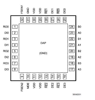
DS91M040: Features: DC - 125 MHz / 250 Mbps low jitter, low skew, low power operation Wide Input Common Mode Voltage Range allows up to ±2V of GND noise Conforms to TIA/EIA-899 M-LVDS Standard Pin selectable...

floor Price/Ceiling Price

Part Number:
DS91M040
Supply Ability:
5000

Price Break

  • Qty
  • 1~5000
  • Unit Price
  • Negotiable
  • Processing time
  • 15 Days
Total Cost: $ 0.00

SeekIC Buyer Protection PLUS - newly updated for 2013!

  • Escrow Protection.
  • Guaranteed refunds.
  • Secure payments.
  • Learn more >>

Month Sales

268 Transactions

Rating

evaluate  (4.8 stars)

Upload time: 2024/4/26

Payment Methods

All payment methods are secure and covered by SeekIC Buyer Protection PLUS.

Notice: When you place an order, your payment is made to SeekIC and not to your seller. SeekIC only pays the seller after confirming you have received your order. We will also never share your payment details with your seller.
Product Details

Description


Features:

DC - 125 MHz / 250 Mbps low jitter, low skew, low power operation
Wide Input Common Mode Voltage Range allows up to ±2V of GND noise
Conforms to TIA/EIA-899 M-LVDS Standard
Pin selectable M-LVDS receiver type (1 or 2)
Controlled transition times (2.0 ns typ) minimize reflections
8 kV ESD on M-LVDS I/O pins protects adjoining components
Flow-through pinout simplifies PCB layout
Small 5 mm x 5 mm LLP-32 space saving package


Application

Multidrop / Multipoint clock and data distribution
High-Speed, Low Power, Short-Reach alternative to TIA/ EIA-485/422
Clock distribution in AdvancedTCA (ATCA) and MicroTCA (TCA) backplane


Pinout

  Connection Diagram


Specifications

Temperature Min -40 deg C
Temperature Max 85 deg C
Function Transceiver
View Using Catalog


Power Supply Voltage −0.3V to +4V
LVCMOS Input Voltage −0.3V to (VDD + 0.3V)
LVCMOS Output Voltage −0.3V to (VDD + 0.3V)
M-LVDS I/O Voltage −5.5V to +5.5V
M-LVDS Output Short Circuit
Current Duration Continuous
Junction Temperature +140°C
Storage Temperature Range −65°C to +150°C
Lead Temperature Range
Soldering (4 sec.) +260°C
Maximum Package Power Dissipation @ +25°C
SQ Package 833 mW
Derate SQ Package 6.67 mW/°C above +25°C
Package Thermal Resistance
JA +150°C/W
JC +63.8°C/W


Description

The DS91M040 is a quad M-LVDS transceiver designed for driving / receiving clock or data signals to / from up to four multipoint networks.

M-LVDS (Multipoint LVDS) is a new family of bus interface devices based on LVDS technology specifically designed for multipoint and multidrop cable and backplane applications. It differs from standard LVDS in providing increased drive current to handle double terminations that are required in multi-point applications. Controlled transition times minimize reflections that are common in multipoint configurations due to unterminated stubs. M-LVDS devices also have a very large input common mode voltage range for additional noise margin in heavily loaded and noisy backplane environments.

A single DS91M040 channel is a half-duplex transceiver that accepts LVTTL/LVCMOS signals at the driver inputs and converts them to differential M-LVDS signal levels. The receiver inputs accept low voltage differential signals (LVDS, BLVDS, M-LVDS, LVPECL and CML) and convert them to 3V LVCMOS signals. The DS91M040 supports both M-LVDS type 1 and type 2 receiver inputs.

Design Tools


Title Size in Kbytes Date
DS91M040EVK Documentation 2 Kbytes 16-Apr-2008 View

If you have trouble printing or viewing PDF file(s), see Printing Problems.

Application Notes


Title Size in Kbytes Date
AN-1926: Application Note 1926 An Introduction to M-LVDS and Clock and Data Distribution Applications 344 Kbytes 4-Dec-08 Download
AN-1503: Application Note 1503 Designing an ATCA Compliant M-LVDS Clock Distribution Network 2926 Kbytes 20-Nov-07 Download
AN-1503 (Chinese): Application Note 1503 Designing an ATCA Compliant M-LVDS Clock Distribution Network
463 Kbytes 640){this.height=this.height*640/this.width;this.width=640;}' border="0" alt=" Connection Diagram">

If you have trouble printing or viewing PDF file(s), see Printing Problems.


Customers Who Bought This Item Also Bought

Margin,quality,low-cost products with low minimum orders. Secure your online payments with SeekIC Buyer Protection.
Undefined Category
Line Protection, Backups
LED Products
Power Supplies - External/Internal (Off-Board)
View more