Features: `Optimized for digital cellular applications with a bit manipulation unit for higher coding efficiency and an error correction coprocessor for equalization and channel coding support.
`On-chip, programmable, PLL clock synthesizer.
`19.2 ns and 12.5 ns instruction cycle times at2.7 V.
`Mask-programmable memory map option: The DSP1628x16 features 16 Kwords on-chip dualport RAM. The DSP1628x08 features 8 Kwords on-chip dual-port RAM. Both feature 48 Kwords on-chip ROM with a secure option.
`Low power consumption:
- <1.9 mW/MIPS typical at 2.7 V.
`Flexible power management modes:
-Standard sleep: 0.2 mW/MIPS at 2.7 V.
-Sleep with slow internal clock: 0.7 mW at 2.7 V.
-Hardware STOP (pin halts DSP): <20mA.
`Mask-programmable clock options: small signal,and CMOS.
`144 PBGA package (13 mm x 13 mm) available.Sequenced accesses to X and Y externalmemory.
`Object code compatible with the DSP1618.
`Single-cycle squaring.
`16 x 16-bit multiplication and 36-bit accumulation in one instruction cycle.
`Instruction cache for high-speed, programefficient,zero-overhead looping.
`Dual 25 Mbit/s serial I/O ports with multiprocessor capability-16-bit data channel, 8-bit protocol channel.
`8-bit parallel host interface
- Supports 8- or 16-bit transfers.
-Motorola*or Intel† compatible.
`8-bit control I/O interface.
`256 memory-mapped I/O ports.
`IEEE‡P1149.1 test port (JTAG boundary scan).
`Full-speed in-circuit emulation hardware development system on-chip.
`Supported by DSP1628 software and hardware development tools.Pinout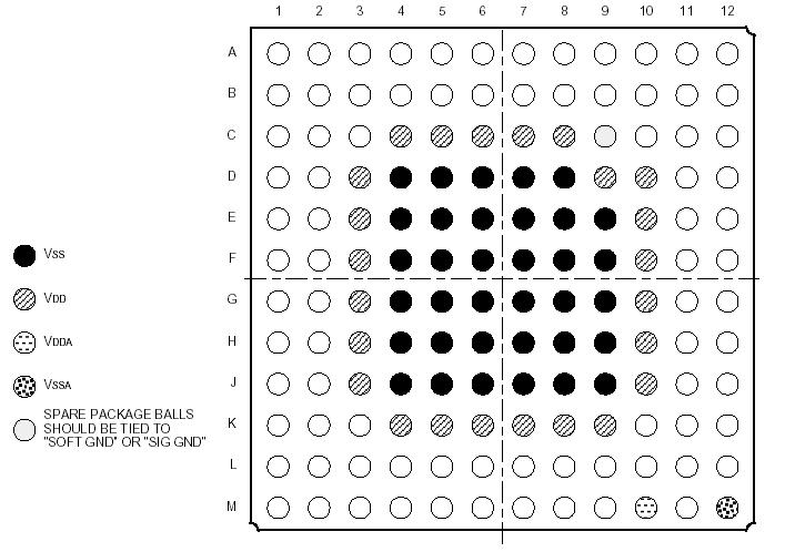 SpecificationsExternal leads can be bonded and soldered safely at temperatures of up to 300 °C......(TBD for 144-pin PBGA)
Voltage Range on VDD with Respect to Ground Using Devices Designed for 3 V Operation ......0.5 V to +4.6 V
Voltage Range on Any Pin ..........................................................................................VSS 0.5 V to VDD + 0.5 V
Power Dissipation..........................................................................................................................................1 W
Ambient Temperature Range ..................................................................................................40 °C to +85 °C
Storage Temperature Range..................................................................................................65 °C to +150 °CDescriptionThe DSP1628 digital signal processor offers 80 MIPS and 52 MIPS operation at 2.7 V. Designed specifically for applications requiring low power dissipation in digital cellular systems, the DSP1628 is a signal-coding device that can be programmed to perform a wide variety of fixed-point signal processing functions. The device is based on the DSP1600 core with a bit manipulation unit for enhanced signal coding effi-ciency, an external memory sequencer, an error correction coprocessor (ECCP) for more efficient Viterbi decoding, and an 8-bit parallel host interface for hardware flexibility. The DSP1628 includes a mix of peripherals specifically intended to support processing-intensive but cost-sensitive applications in the area of digital wireless communications.
The DSP1628x16 contains 16 Kwords of internal dual-port RAM (DPRAM), which allows simultaneous access to two RAM locations in a single instruction cycle.
The DSP1628x08 supports the use of 8 Kwords of DPRAM. Both devices contain 48 Kwords of internal ROM (IROM).
The DSP1628 is object code compatible with the DSP1618, while providing more memory. The DSP1628 is pin compatible with the DSP1627. Note that TRST (JTAG test reset), replaces a V DD pin.
The DSP1628 supports 2.7 V operation with flexible power management modes required for portable cellular terminals. Several control mechanisms achieve low-power operation, including a STOP pin for placing the DSP into a fully static, halted state and a programmable power control register used to power down unused on-chip I/O units. These power management modes allow for trade-offs between power reduction and wake-up latency requirements. During system standby, power consumption is reduced to less than 20mA.
The DSP1628 on-chip clock synthesizer can be driven by an external clock whose frequency is a fraction of the instruction rate.
The DSP1628 device is packaged in a 144-pin PBGA, a 100-pin BQFP, or a 100-pin TQFP and is available with 19.2 ns and 12.5 ns instruction cycle times at 2.7 V.

 DSP1629 Data Sheet