Features: • Program control unit (PCU)
• DMA controller (with six channels)
• Instruction patch controller
• PLL-based clock oscillator
• OnCE module
• MemoryPinout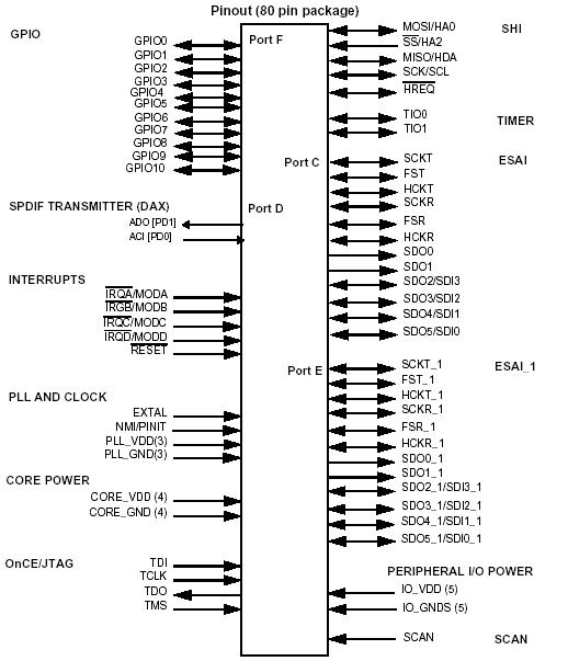 Specifications
| Rating1 |
Symbol |
Value1, 2 |
Unit |
| All "5.0V tolerant" input voltages |
VIN |
GND − 0.3 to 5.5V |
V |
Current drain per pin excluding VDD and GND
(Except for pads listed below) |
I |
12 |
mA |
| SCK_SCL |
ISCK |
16 |
mA |
| ACI_PD0,ADO_PD1 |
IDAX |
24 |
mA |
| TDO |
Ijtag |
24 |
mA |
| Operating temperature range3 |
TJ |
-40 to +115 |
°C |
| Storage temperature |
TSTG |
−55 to +125 |
°C |
DescriptionThe DSP56371 uses the DSP56300 core, a high-performance, single clock cycle per instruction engine that provides up to twice the performance of Motorola's popular DSP56000 core family while retaining code compatibility with it.
The DSP56300 core family offers a new level of performance in speed and power, provided by its rich instruction set and low power dissipation, thus enabling a new generation of wireless, telecommunications and multimedia products. For a description of the DSP56300 core, see Section 2.4 DSP56300 Core Functional Blocks. Significant architectural enhancements to the DSP56300 core family include a barrel shifter, 24-bit addressing, an instruction patch module and direct memory access (DMA).
The DSP56300 core family members contain the DSP56300 core and additional modules. The modules are chosen from a library of standard predesigned elements such as memories and peripherals. New modules may be added to the library to meet customer specifications. A standard interface between the DSP56300 core and the on-chip memory and peripherals supports a wide variety of memory and peripheral configurations. Refer to DSP56371 User Manual, Section 3, Memory Configuration. Core features are described fully in the DSP56300 Family Manual. Pinout, memory and peripheral features are described in this manual.

 DSP56371 Data Sheet