Features: • Choose among the following memory organizations: Commercial
V-III Vx-III
IDT72V15160 - 4,096 x 16 IDT72V14320 - 1,024 x 32
IDT72V16160 - 8,192 x 16 IDT72V15320 - 2,048 x 32
IDT72V17160 - 16,384 x 16 IDT72V16320 - 4,096 x 32
IDT72V18160 - 32,768 x 16 IDT72V17320 - 8,192 x 32
IDT72V19160 - 65,536 x 16 IDT72V18320 - 16,384 x 32
IDT72V19320 - 32,768 x 32
• Up to 100 MHz Operation of the Clocks
• 5V input tolerant
• Auto power down minimizes standby power consumption
• Master Reset clears entire FIFO
• Partial Reset clears data, but retains programmable settings
• Empty, Full and Half-Full flags signal FIFO status
• Programmable Almost-Empty and Almost-Full flags, each flag can default to one of eight preselected offsets
• Program programmable flags through serial input
• Output enable puts data outputs into high impedance state
• JTAG port, provided for Boundary Scan function (PBGA Only)
• Available in a 80-pin (V-III) Thin Quad Flat Pack, 128-pin(Vx-III)
Thin Quad Flat Pack (TQFP) or a 144-pin (Vx-III) Plastic Ball Grid
Array (PBGA) (with additional features)
• Industrial temperature range (40°C to +85°C)
• High-performance submicron CMOS technologyPinout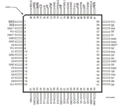 Specifications
| Symbol |
Rating |
Commercial
|
Unit |
| VTERM(2) |
Terminal Voltage with Respect to GND |
0.5 to +4.5 |
V |
| TSTG |
Storage Temperature |
55 to +125 |
|
| IOUT |
DC Output Current |
50 to +50 |
mA |
NOTES:
1. Stresses greater than those listed under ABSOLUTE MAXIMUM RATINGS may cause permanent damage to the device. This is a stress rating only and functional operation of the device at these or any other conditions above those indicated in the operational sections of this specification is not implied. Exposure to absolute maximum rating conditions for extended periods may affect reliability.
2. VCC terminal only.DescriptionThe DT72V18160 IDT V-III and Vx-III Multimedia FIFOs are exceptionally deep, high speed, CMOS First-In-First-Out (FIFO) memories with independent clocked read and write controls and high density offerings up to 1 Mbit.
Each DT72V18160 FIFO has a data input port (Dn) and a data output port (Qn). The frequencies of both the RCLK (read port clock) and the WCLK (write port clock) signals may vary from 0 to fS(MAX) with complete independence. There are no restrictions on the frequency of the one clock input with respect to the other.
These DT72V18160 FIFOs have five flag pins, EF (Empty Flag), FF (Full Flag), HF (Halffull Flag), PAE (Programmable Almost-Empty flag) and PAF (Programmable Almost-Full flag).
DT72V18160 PAE and PAF can be programmed independently to switch at any point in memory. Programmable offsets determine the flag switching threshold and can be loaded with the serial interface to any user desired value or by default values. Eight default offset settings are provided, so that PAE can be set to switch at a predefined number of locations from the empty boundary and the PAF threshold can also be set at similar predefined values from the full boundary. The default offset values are set during Master Reset by the state of the FSEL0, FSEL1, and LD pins.
For serial programming, DT72V18160 SEN together with LD on each rising edge of WCLK, are used to load the offset registers via the Serial Input (SI). During Master Reset (MRS) the read and write pointers are set to the first location of the FIFO.
The DT72V18160 Partial Reset (PRS) also sets the read and write pointers to the first location of the memory. However, the programmable flag settings existing before Partial Reset remain unchanged. PRS is useful for resetting a device in midoperation, when reprogramming programmable flags would be undesirable.
DT72V18160 is also possible to select the timing mode of the PAE (Programmable Almost- Empty flag) and PAF (Programmable Almost-Full flag) outputs. The timing modes can be set to be either asynchronous or synchronous for the PAE and PAF flags.
If asynchronous PAE/PAF configuration is selected, the PAE is asserted LOW on the LOW-to-HIGH transition of RCLK. PAE is reset to HIGH on the LOWto- HIGH transition of WCLK. Similarly, the PAF is asserted LOW on the LOWto- HIGH transition of WCLK and PAF is reset to HIGH on the LOW-to-HIGH transition of RCLK.
If DT72V18160 synchronousPAE/PAF configuration is selected , the PAE is asserted and updated on the rising edge of RCLK only and not WCLK. Similarly,PAF is asserted and updated on the rising edge of WCLK only and not RCLK. The mode desired is configured during Master Reset by the state of the Programmable Flag Mode (PFM) pin.
If, at any time, the FIFO DT72V18160 is not actively performing an operation, the chip will automatically power down. Once in the power down state, the standby supply current consumption is minimized. Initiating any operation (by activating control inputs) will immediately take the device out of the power down state.
The DT72V18160 IDT V-III and Vx-III family of FIFOs are fabricated using IDT's high speed submicron CMOS technology.

 DT72V18160 Data Sheet


