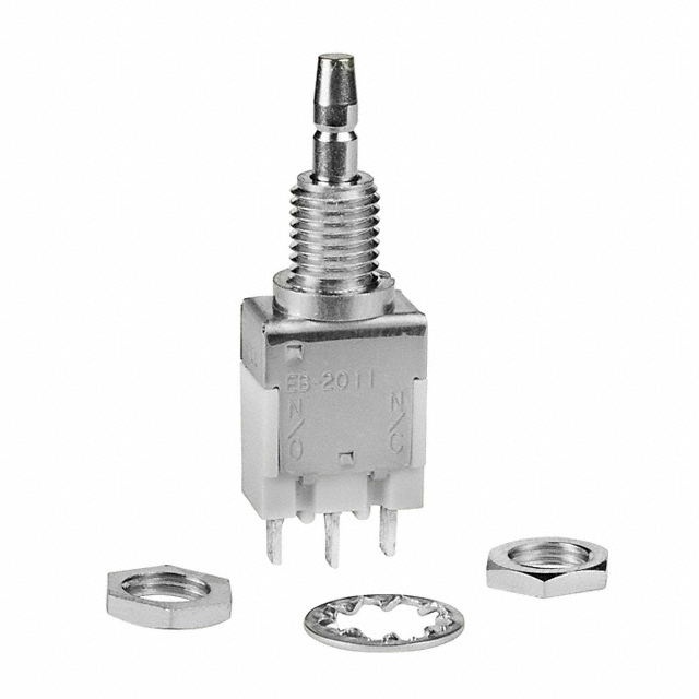
EB200P70-AJ

Features: • 20 dBm Output Power (P1dB)• 17 dB Gain at 5.8 GHz• 0.7 dB Noise Figure at 5.8 GHz• 30 dBm Output IP3• 45% Power-Added Efficiency• Useable Gain to 26 GHzApplication• LNAs and Driver Amplifiers to 26GHz• VCOs and Frequency DoublersSpecifica...

product image

EB200P70-AJ Picture
SeekIC No. : 004330840 Detail

EB200P70-AJ: Features: • 20 dBm Output Power (P1dB)• 17 dB Gain at 5.8 GHz• 0.7 dB Noise Figure at 5.8 GHz• 30 dBm Output IP3• 45% Power-Added Efficiency• Useable Gain to 26 G...

floor Price/Ceiling Price

Part Number:
EB200P70-AJ
Supply Ability:
5000

Price Break

  • Qty
  • 1~5000
  • Unit Price
  • Negotiable
  • Processing time
  • 15 Days
Total Cost: $ 0.00

SeekIC Buyer Protection PLUS - newly updated for 2013!

  • Escrow Protection.
  • Guaranteed refunds.
  • Secure payments.
  • Learn more >>

Month Sales

268 Transactions

Rating

evaluate  (4.8 stars)

Upload time: 2024/4/26

Payment Methods

All payment methods are secure and covered by SeekIC Buyer Protection PLUS.

Notice: When you place an order, your payment is made to SeekIC and not to your seller. SeekIC only pays the seller after confirming you have received your order. We will also never share your payment details with your seller.
Product Details

Description


Features:

• 20 dBm Output Power (P1dB)
• 17 dB Gain at 5.8 GHz
• 0.7 dB Noise Figure at 5.8 GHz
• 30 dBm Output IP3
• 45% Power-Added Efficiency
• Useable Gain to 26 GHz


Application

• LNAs and Driver Amplifiers to 26GHz
• VCOs and Frequency Doublers


Specifications

PARAMETER SYMBOL TEST CONDITIONS ABSOLUTE MAXIMUM
Drain-Source Voltage VDS -3V < VGS < -0.5V 8V
Gate-Source Voltage VGS 0V < VDS < +8V -3V
Drain-Source Current IDS For VDS > 2V IDSS
Gate Current IG Forward or reverse current 5mA
RF Input Power2 PIN Under any acceptable bias state 16dBm
Channel Operating Temperature TGH Under any acceptable bias state 175°C
Storage Temperature TSTG Non-Operating Storage -40°C to 150°C
Total Power Dissipation PTOT See De-Rating Note below 470mW
Simultaneous Combination of Limits4   2 or more Max. Limi 80%
1TAmbient = 22°C unless otherwise noted; exceeding any one of these absolute maximum ratings may cause permanent damage to the device
2Max. RF Input Limit must be further limited if input VSWR > 2.5:1
3Users should avoid exceeding 80% of 2 or more Limits simultaneously
4Total Power Dissipation defined as: PTOT (PDC + PIN) POUT,
where PDC: DC Bias Power, PIN: RF Input Power, POUT: RF Output Power
Total Power Dissipation to be de-rated as follows above 22°C:
PTOT= 0.47 - (1/RJC) x TPACK
where TPACK= source tab lead temperature above 22°C
(coefficient of de-rating formula is the Thermal Conductivity)
Example: For a 65°C carrier temperature: PTOT = 470mW (3 x (65 22)) = 341mW


Description

The FPD200P70 is a packaged depletion mode AlGaAs/InGaAs pseudomorphic High Electron Mobility Transistor (pHEMT). It utilizes a 0.25 mm x 200 mm Schottky barrier Gate, defined by high-resolution stepper-based photolithography.


Customers Who Bought This Item Also Bought

Margin,quality,low-cost products with low minimum orders. Secure your online payments with SeekIC Buyer Protection.
Power Supplies - Board Mount
Line Protection, Backups
Boxes, Enclosures, Racks
Batteries, Chargers, Holders
Memory Cards, Modules
View more