|
Nominal Frequency | 50.000MHz, 51.840MHz, 52.000MHz, 52.080MHz, 54.000MHz, 57.1429MHz, 61.440MHz, 63.360MHz, 65.536MHz, 76.800MHz, 77.760MHz, 100.000MHz, 104.000MHz, 106.250MHz, 125.000MHz, 126.720MHz, 128.000MHz, 153.600MHz, 155.520MHz, 156.250MHz, 159.375MHz, 161.1328MHz, 166.6286MHz, 167.3315MHz, 184.320MHz, or 186.666MHz |
The specified reference or "center" frequency of the oscillator. Typically specified in megahertz (MHz)or kilohertz (kHz). |
|
| Frequency Tolerance/Stability | Inclusive of all conditions: Calibration Tolerance at 25°C, Frequency Stability over the Operating Temperature Range, Supply Voltage Change, Output Load Change, 1st Year Aging at 25°C, Shock, and Vibration
±50ppm Maximum
±25ppm Maximum |
|
Operating Temperature Range | 0°C to +70°C
-40°C to +85°C |
The maximum and minimum temperatures that the oscillator device can be exposed to during oscillation. Over thistemperature range, all of the specified device operatingparameters are guaranteed. |
|
Supply Voltage (VCC) | 3.3VDC ±5% |
The DC input voltage necessary for oscillator operation, specified involts. |
|
Input Current | 80mA Maximum |
The amount of current consumption by an oscillator from the powersupply, typically specified in milliamps (mA). |
|
| Output Voltage Logic High (VOH) | 1.43VDC Typical, 1.6VDC Maximum |
|
| Output Voltage Logic Low (VOL) | 1.1VDC Typical, 0.9VDC Maximum |
|
| Differential Output Voltage (VOD) | 247mV Minimum, 355mV Typical, 454mV Maximum |
|
| VDD Magnitude Change (DVDD) | -50mV Minimum, +50mV Maximum |
|
| Offset Voltage (VOS) | 1.125V Minimum, 1.20V Typical, 1.375V Maximum |
|
| Offset Voltage Magnitude Change (DVOS) | 25mV Maximum |
|
Duty Cycle | Measured at 50% of waveform
50 ±10(%)
50 ±5(%) |
The measure of output waveform uniformity. This term, also referredto as symmetry, is a measurement of the time that the outputwaveform is in a logic high state, expressed as a percentage (%).This parameter is measured at a specified voltage threshold or at apercentage of the output waveform amplitude (Figure 1 in the oscillator glossary of terms). |
|
Rise Time/Fall Time | Measured over 20% to 80% of waveform
1nSec Maximum |
The Rise Time, measured in nanoseconds (nSec), is defined as thetransition time from an output logic low to an output logic high.Conversely, the Fall Time, also measured in nanoseconds (nSec), isdefined as the transition time from an output logic high to an outputlogic low. This transition time is measured at specified voltagethresholds or at specified percentages of the output waveformamplitude (Figure 1 in the oscillator glossary of terms). |
|
| Load Drive Capability | 100 Ohms and 10pF Between Output and Complementary Output |
|
Storage Temperature | -55°C to +125°C |
The minimum and maximum temperatures that the device can be stored or exposed to when in a non-oscillation state. After exposing or storing the device at the minimum or maximum temperatures for a length of time, all of the operating specifications are guaranteed over the specified Operating Temperature Range. |
|
| Control Voltage (VC) | 1.65VDC ±1.65VDC (Test condition for frequency deviation) |
|
| Control Voltage Range (VCR) | 0.0VDC to VCC +0.5VDC |
|
| Frequency Deviation | Inclusive of Operating Temperature Range, Supply Voltage Change, and Output Load Change
±75ppm Minimum |
|
| Linearity | 20% Maximum
15% Maximum
10% Maximum |
|
| Transfer Function | Positive Transfer Characteristic |
|
| Modulation Bandwidth (MBW) | 10kHz Minimum (Measured at -3dB with Control Voltage of +1.65VDC |
|
| Input Impedance (ZI) | 50kOhms Typical |
|
| Logic Control / Additional Output | Tri-State (Enable High) / Complementary Output |
|
| Tri-State Input Voltage | VIH of 70% of VCC Minimum or No Connect to Enable Output and Complementary Output, VIL of 30% of VCC Maximum to Disable Output and Complementary Output (High Impedance). |
|
| Start-Up Time | 10mSec Maximum |
|
| RMS Phase Jitter | 0.4pSec Typical, 1pSec Maximum (FJ=12kHz to 20MHz) |
|
| Accumulated Period Jitter (tACC) | 4pSec Typical, 5pSec Maximum (Sigma of Total Jitter Distribution) |
|
| Period Jitter (tRJ) | 3pSec Typical, 5pSec Maximum (Sigma of Random Jitter) |
|
| Period Jitter (tRMS) | 3pSec Typical, 5pSec Maximum (Sigma of Total Jitter Distribution) |
|
| Period Jitter (tDJ) | 4pSec Typical, 10pSec Maximum (Deterministic Jitter) |
|
| Period Jitter (tP-P) | 27pSec Typical, 40pSec Maximum (Peak-to-Peak of Jitter Distribution) |
|
| Phase Noise | Typical Values, FO = 155.520MHz
-55dBc/Hz at 10Hz Offset
-90dBc/Hz at 100Hz Offset
-120dBc/Hz at 1kHz Offset
-140dBc/Hz at 10kHz Offset
-145dBc/Hz at 100kHz Offset
-148dBc/Hz at 1MHz Offset |
|

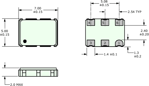
 EL32D1 Data Sheet