DescriptionThe EM48BM1684LBA_09 is one member of the EM48BM1684LBA series.The EM48BM1684LBA is Synchronous Dynamic Random Access Memory (SDRAM) organized as 8Meg words x 4 banks by 16 bits. All inputs and outputs are synchronized with the positive edge of the clock.The 512Mb SDRAM uses synchronize...
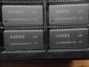
EM48BM1684LBA_09: DescriptionThe EM48BM1684LBA_09 is one member of the EM48BM1684LBA series.The EM48BM1684LBA is Synchronous Dynamic Random Access Memory (SDRAM) organized as 8Meg words x 4 banks by 16 bits. All inpu...
SeekIC Buyer Protection PLUS - newly updated for 2013!
268 Transactions
All payment methods are secure and covered by SeekIC Buyer Protection PLUS.
DescriptionThe EM481M1622VTC is Synchronous Dynamic Random Access Memory (SDRAM) organized as 512K...
DescriptionThe EM484M1644VTA is Synchronous Dynamic Random Access Memory (SDRAM) organized as 1Meg...
The EM48BM1684LBA_09 is one member of the EM48BM1684LBA series.The EM48BM1684LBA is Synchronous Dynamic Random Access Memory (SDRAM) organized as 8Meg words x 4 banks by 16 bits. All inputs and outputs are synchronized with the positive edge of the clock.The 512Mb SDRAM uses synchronized pipelined architecture to achieve high speed data transfer rates and is designed to operate at 1.8V low power memory system. It also provides auto refresh with power saving / down mode. All inputs and outputs voltage levels are compatible with LVCMOS.
Features of the EM48BM1684LBA_09 are:(1)fully synchronous to positive clock edge; (2)LVCMOS compatible with multiplexed address; (3)programmable burst length (B/L) - 1, 2, 4, 8 or full page; (4)programmable CAS latency (C/L) - 2 or 3; (5)Data Mask (DQM) for Read / write masking; (6)burst read with single-bit write operation; (7)all inputs are sampled at the rising edge of the system clock; (8)auto refresh and self refresh; (9)8,192 refresh cycles / 64ms (7.8us); (10)partial array self-refresh (PASR); (11)driver strength: normal/weak.
The absolute maximum ratings of the EM48BM1684LBA_09 can be summarized as:(1)storage temperature range:-55 to 125;(2)operating temperature range:0 to 70;(3)input,output voltage range:-0.3 to 2.3V;(4)power supply voltage:-0.3 to 2.3V;(5)power dissipation:1W;(6)short circuit current:50mA.Caution Exposing the device to stress above those listed in Absolute Maximum Ratings could cause permanent damage. The device is not meant to be operated under conditions outside the limits described in the operational section of this specification. Exposure to Absolute Maximum Rating conditions for extended periods may affect device reliability.To prevent data contention on the DQ bus during power on, it is required that the DQM and CKE pins be held high during the initial pause period. Once all banks have been precharged, the Mode Register Set Command must be issued to initialize the Mode Register. A minimum of eight Auto Refresh cycles (CBR) are also required, and these may be done before or after programming the Mode Register.