FLASH MEMORY

Features: • Seven erase blocks:16KB/8K-word boot block (protected)Two 8KB/4K-word parameter blocksFour main memory blocks• Smart 3 technology (B3):3.3V ±0.3V VCC3.3V ±0.3V VPP application programming5V ±10% VPP application/production programming1• Compatible with 0.3µm Smar...

product image

FLASH MEMORY Picture
SeekIC No. : 004341968 Detail

FLASH MEMORY: Features: • Seven erase blocks:16KB/8K-word boot block (protected)Two 8KB/4K-word parameter blocksFour main memory blocks• Smart 3 technology (B3):3.3V ±0.3V VCC3.3V ±0.3V VPP applicatio...

floor Price/Ceiling Price

Part Number:
FLASH MEMORY
Supply Ability:
5000

Price Break

  • Qty
  • 1~5000
  • Unit Price
  • Negotiable
  • Processing time
  • 15 Days
Total Cost: $ 0.00

SeekIC Buyer Protection PLUS - newly updated for 2013!

  • Escrow Protection.
  • Guaranteed refunds.
  • Secure payments.
  • Learn more >>

Month Sales

268 Transactions

Rating

evaluate  (4.8 stars)

Upload time: 2024/4/28

Payment Methods

All payment methods are secure and covered by SeekIC Buyer Protection PLUS.

Notice: When you place an order, your payment is made to SeekIC and not to your seller. SeekIC only pays the seller after confirming you have received your order. We will also never share your payment details with your seller.
Product Details

Description


Features:


• Seven erase blocks:
16KB/8K-word boot block (protected)
Two 8KB/4K-word parameter blocks
Four main memory blocks
• Smart 3 technology (B3):
3.3V ±0.3V VCC
3.3V ±0.3V VPP application programming
5V ±10% VPP application/production programming1
• Compatible with 0.3µm Smart 3 device
• Advanced 0.18µm CMOS floating-gate process
• Address access time: 80ns
• 100,000 ERASE cycles
• Industry-standard pinouts
• Inputs and outputs are fully TTL-compatible
• Automated write and erase algorithm
• Two-cycle WRITE/ERASE sequence
• Byte- or word-wide READ and WRITE
(MT28F400B3, 256K x 16/512K x 8)
• Byte-wide READ and WRITE only
(MT28F004B3, 512K x 8)
• TSOP and SOP packaging options


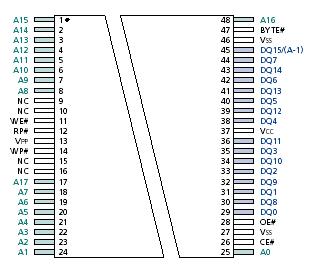
Pinout

  Connection Diagram


Specifications

Voltage on VCC Supply
Relative to VSS ..........................................-0.5V to +4V**
Input Voltage Relative to VSS ....................-0.5V to +4V**
VPP Voltage Relative to VSS ......................-0.5V to +5.5V
RP# or A9 Pin Voltage
Relative to VSS ......................................-0.5V to +12.6V††
Temperature Under Bias .......................... -40ºC to +85ºC
Storage Temperature (plastic) ............... -55ºC to +125ºC
Power Dissipation .........................................................1W


Description

The MT28F004B3 (x8) and MT28F400B3 (x16/x8) are nonvolatile, electrically block-erasable (flash), programmable memory devices containing 4,194,304 bits organized as 262,144 words (16 bits) or 524,288 bytes (8 bits). Writing or erasing the MT28F004B3 and MT28F400B3 is done with either a 3.3V or 5V VPP voltage, while all operations are performed with a 3.3V VCC. Due to process technology advances, 5V VPP is optimal for application and production programming. These devices are fabricated with Micron's advanced 0.18µm CMOS floating-gate process.

The MT28F004B3 and MT28F400B3 are organized into seven separately erasable blocks. To ensure that critical firmware is protected from accidental erasure or overwrite, the MT28F004B3 and MT28F400B3 feature a hardware-protected boot block. Writing or erasing the boot block requires either applying a super-voltage to the RP# pin or driving WP HIGH in addition to executing the normal write or erase sequences. This block may be used to store code implemented in low-level system recovery. The remaining blocks vary in density and are written and erased with no additional security measures.


Customers Who Bought This Item Also Bought

Margin,quality,low-cost products with low minimum orders. Secure your online payments with SeekIC Buyer Protection.
Audio Products
Hardware, Fasteners, Accessories
LED Products
Isolators
Connectors, Interconnects
Industrial Controls, Meters
View more