Features: ` Voltage level shifting
` 4 switch connection between two ports
` Minimal propagation delay through the switch
` Low lCC
` Zero bounce in flow-through mode
` Control inputs compatible with TTL level
` Packaged in plastic Fine-Pitch Ball Grid Array (FBGA) (Preliminary)ApplicationSelect pins S0, S1, S2, S3, S4 and S5 are intended to be used as static user configurable control pins. The AC performance of these pins has not been characterized or tested. Switching of these select pins during system operation may temporarily disrupt output logic states and/or enable pin controls.
40-bit configuration can be achieved by connecting the OE1 and the OE6 pins to together
Pinout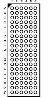 Specifications
Supply Voltage (VCC) .................................−0.5V to +7.0V
DC Switch Voltage (VS) (Note 3) ................−2.0V to +7.0V
DC Input Control Pin Voltage
(VIN) (Note 4) ............................................−0.5V to +7.0V
DC Input Diode Current (lIK) VIN < 0V.................. −50 mA
DC Output (IOUT) Current..................................... 128 mA
DC VCC/GND Current (ICC/IGND) ....................+/− 100 mA
Storage Temperature Range (TSTG)..... −65°C to +150 °C
DescriptionThe Fairchild Universal Bus Switch FSTD32450 provides 4-bit, 5-bit, 8-bit, 10-bit, 16-bit, 20-bit...40-bit of high-speed CMOS TTL-compatible bus switching. The low On Resistance of the switch allows inputs to be connected to outputs without adding propagation delay or generating additional ground bounce noise.
The FSTD32450 is designed to allow "customer" configuration control of the enable connections. The device can be organized as either a ten 4-bit, eight 5-bit, four 10-bit, two 20-bit or one 40-bit enabled bus switch. Also achievable are 8-bit and 16-bit enabled configurations (see Functional Description). The FSTD32450's bit configuration is controlled through select pin logic. (see Truth Table). When OEx is LOW, Port Ax is connected to Port Bx. When OEx is HIGH, the switch is OPEN.
Another key FSTD32450 feature is the addition of a level shifting select pin, "S2 and S5". When S2 and S5 are LOW, the device behaves as a standard N-MOS switch. When S2 and S5 are HIGH, a diode to VCC is integrated into the circuit allowing for level shifting between 5V inputs and 3.3V
outputs.

 FSTD32450 Data Sheet


