Features: 80 million samples per second input rate
0.1 Hz tuning resolution
>75 dB dynamic range
Programmable output bandwidth
12 bit inputs, 10, 12, 14, or 16 bit outputs
Real or complex output formats
Built in strobe/sync generator
Symmetric rounding used throughout
Gain adjust in 0.03 dB steps
Microprocessor interface for control,output, and diagnostics
Power down mode
Auto power down with clock loss detection
Built in diagnostics
3.25W power at 50 MHz, 5 volts
850 mW at 30 MHz, 3.3 volts
120 pin quad flat pack packagePinout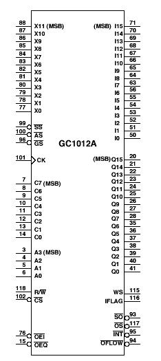 Specifications
| PARAMETER |
SYMBOL |
MIN |
MAX |
UNITS |
NOTES |
| DC Supply Voltage |
VCC |
-0.3 |
7 |
V |
|
| Input voltage (undershoot and overshoot) |
VIN |
-0.7 |
VCC+0.7 |
V |
|
| Storage Temperature |
TSTG |
-65 |
150 |
°C |
|
| Lead Soldering Temperature (10 seconds) |
|
|
300 |
°C |
|
| Clock Rate |
FCK |
1 |
|
KHz |
1 |
Description Fabricated in high speed CMOS technology, the GC1012A chip is an all digital tuner which can downconvert and band limit signals from wide band digitized sources. At full rate operation of GC1012A (80 MHz input rate), the input bandwidth can be up to 40 MHz wide. Any signal within the input bandwidth can be down-converted to zero frequency, low pass filtered, and output at a reduced sample rate. The chipÕs output of GC1012A can be formatted as either a complex data stream, or as a real data stream. The complex samples are output at rates equal to F
O=F
CK/D, where F
O is the output rate, D is 1, 2, 4, 8, 16, 32 or 64 and F
CK is the input sample (clock) rate. The real output rates are F
O=2F
CK /D for D equal to 2, 4, 8, 16, 32, or 64.
The signal of GC1012A is low pass filtered to remove out of band energy before the sample rate is decreased. The filterÕs out of band rejection is over 75 dB and its passband ripple is less than 0.2 dB peak to peak. The passband of the output filter covers 80% of the output bandwidth.
The 28 bit accumulator in the chipÕs digital oscillator circuit provides a tuning accuracy equal to the input clock rate divided by 2
28. The tuning resolution at a clock rate of 50 MHz is less than 0.2 Hz giving a tuning accuracy of +/- 0.1 Hz. The phase noise in the oscillator is low enough to provide a spur free dynamic range of over 75 dB.
The chips output circuit of GC1012A allows the user to select a real or complex data output format, to select spectral inversion, or to offset the output spectrum by half of the output sample rate. The outputs signal gain of GC1012A can be adjusted in 0.03 dB steps. The word size of the output samples are either 10, 12, 14, or 16 bits.
On chip diagnostic circuits of GC1012A are provided to simplify system debug and maintenance.
The chip of GC1012A receives configuration and control information over a microprocessor compatible bus consisting of an 8 bit data I/O port, a 4 bit address port, a read/write bit, and a control select strobe.
I and Q output registers of GC1012A can be read from the control port to allow an external processor to monitor or process the chipÕs output samples. These registers are valuable for monitoring the chipÕs output power in order to set and adjust gain levels.

 GC1012A Data Sheet


