PinoutDescriptionThe GD75232DB is designed as one kind of multiple RS-232 drivers and receivers which combines three drivers and five receivers from TIE trade-standard SN75188 and SN75189 bipolar quadruple drivers and receivers, respectively. The pinout matches the flow-through design of the SN75C...
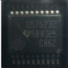
GD75232DB: PinoutDescriptionThe GD75232DB is designed as one kind of multiple RS-232 drivers and receivers which combines three drivers and five receivers from TIE trade-standard SN75188 and SN75189 bipolar qu...
SeekIC Buyer Protection PLUS - newly updated for 2013!
268 Transactions
All payment methods are secure and covered by SeekIC Buyer Protection PLUS.
The GD75232DB is designed as one kind of multiple RS-232 drivers and receivers which combines three drivers and five receivers from TIE trade-standard SN75188 and SN75189 bipolar quadruple drivers and receivers, respectively. The pinout matches the flow-through design of the SN75C185 to decrease the part count, reduce the board space required, and allow easy interconnection of the UART and serial-port connector of an IBME PC/ATE and compatibles.
GD75232DB has six features. (1)Single chip with easy interface between UART and serial-port connector of IBME PC/ATE and compatibles. (2)Meets or exceeds the requirements of ANSI standard TIA/EIA-232-F and ITU recommendation V.28. (3)Designed to support data rates up to 120kbit/s. (4)Pinout compatible with SN75C185 and SN75185. (5)ESD protection to 2kV on bus terminals. (6)Package options is shrink small-outline (DB) packages. those are all the main features.
Some absolute maximum ratings of GD75232DB have been concluded into several points as follow. (1)Its supply voltage Vcc would be 10V. (2)Its supply voltage Vdd would be 15V. (3)Its supply voltage Vss would be -15V. (4)Its input voltage range which would be from -15V to 7V for driver and would be from -30V to 30V for receiver. (5)Its driver output voltage range would be from -15V to 15V. (6)Its receiver low-level output current would be 20mA. (7)Its package thermal impedance would be 115°C/W. (8)Its storage temperature range would be from -65°C to 150°C. (9)Its lead temperature 1.6mm (1/16inch) from case for 10 seconds would be 260°C. It should be noted that stresses above those listed in absolute maximum ratings may cause permanent damage to device.
Also some electrical characteristics of GD75232DB are concluded as follow. (1)Its high level output voltag would be min 6V and typ 7.5V. (2)Its low level output voltage would be typ -7.5V and max -6V. (3)Its high level input current would be max 10uA. (4)Its low level input current would be max -1.6mA. And so on. If you have any question or suggestion or want to know more information about GD75232DB please contact us for details. Thank you!