Features: • Low output impedance ( typical 35Ω at VIN = 5V )
• Low quiescent current ( typical 36µA at VIN = 5V)
• High power conversion efficiency ( typical 98% )
• Simple and accurate voltage conversion from
positive to negative polarities
• Improved latch-up protection
• No external diodes requiredApplication• 5V supply from + 5V logic supply
• EIA/TIA 232E and EIA/TIA 562 power supplies
• Portable telephones
• Data acquisition systems
• Personal communications equipment
• Panel meters
• Handheld instruments Pinout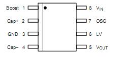 Specifications
| Parameter |
Symbol |
Value |
Unit |
| Supply Voltage (VIN to GND) |
VIN |
6.0 |
V |
| Input Voltage (Pin 1, 6 and 7) |
VIN |
0.3V VIN (VIN, +0.3V) |
V |
| LV Input Current |
LV1 |
20 |
µA |
| Output Short Circuit Duration |
|
Continuous |
|
| Operating Junction Temperature Range |
TJ |
40 to +125 |
°C |
| Storage Temperature Range |
TS |
65 to +150 |
°C |
Continuous Power Dissipation
Plastic Dip (Derate 7.9mW/°C above 70°C) SO-8 (Derate 6mW/°C above 70°C) |
PD |
630
480 |
mW |
DescriptionThe GS7660 is a monolithic CMOS switched capacitor voltage converter, designed to be an improved direct replacement of the popular ICL7660, MAX1044 and LTC1044. They perform supply voltage conversions from positive to negative for an input voltage range of +1.5V to +6.0V to their negative complements of 1.5V to 6.0V. The input voltage of GS7660 can also be doubled (VOUT = 2VIN), halved (VOUT = VIN/2), or multiplied (VOUT = ± n.VIN).
Contained on the chip of GS7660 are a series Power Supply regulator, Oscillator, control Circuitry and four Power MOS Switches. The oscillator, when unloaded, oscillates at a nominal frequency of 10 kHz, with an Input voltage of 5.0V. This frequency of GS7660 can be lowered by the addition of an external capacitor to the "Osc" terminal or overdriven by an external frequency source.
An Oscillator "boost" function of GS7660 is available to increase the oscillator frequency which will optimize performance of certain parameters. The Lv input can be connected to ground to improve low voltage operation (VIN 3V), or left open for input voltages greater than 3V to reduce power dissipation.
The GS7660 provides superior performance over earlier designs by combining low output impedance and low qui- escent current with high efficiency and by eliminating diode voltage drop losses. The only external components required are two low cost electrolytic capacitors.

 GS7660 Data Sheet


