Features: • 256K x 18 and 128K x 36 configurations
• User configurable Pipeline and Flow Through mode
• NBT (No Bus Turn Around) functionality allows zero wait read-write-read bus utilization
• Fully pin compatible with both pipelined and flow through NtRAM™, NoBL™ and ZBT™ SRAMs
• Pin-compatible with 2M, 8M and 16M devices
• 3.3 V +10%/5% core power supply
• 2.5 V or 3.3 V I/O supply
• LBO pin for Linear or Interleave Burst mode
• Byte write operation (9-bit Bytes)
• 3 chip enable signals for easy depth expansion
• Clock Control, registered address, data, and control
• ZZ Pin for automatic power-down
• JEDEC-standard 100-lead TQFP package
• Pb-Free 100-lead TQFP package availablePinout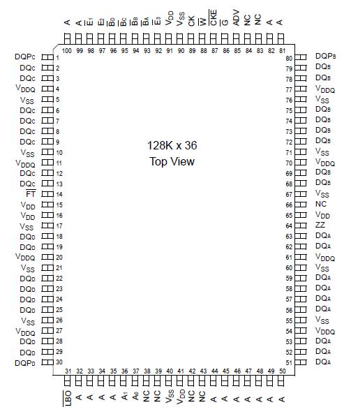
Specifications
| Symbol |
Description |
Value |
Unit |
| VDD |
Voltage on VDD Pins |
0.5 to 4.6 |
V |
| VDDQ |
Voltage in VDDQPins |
0.5 to 4.6 |
V |
| VI/O |
Voltage on I/O Pins |
0.5 to VDDQ+0.5 ( 4.6 V max.) |
V |
| VIN |
Voltage on Other Input Pins |
0.5 to VDD +0.5 ( 4.6 V max.) |
V |
| IIN |
Input Current on Any Pin |
+/20 |
mA |
| IOUT |
Output Current on Any I/O Pin |
+/20 |
mA |
| PD |
Package Power Dissipation |
1.5 |
W |
| TSTG |
Storage Temperature |
55 to 125 |
|
| TBIAS |
Temperature Under Bias |
55 to 125 |
|
Note:
Permanent damage to the device may occur if the Absolute Maximum Ratings are exceeded. Operation should be restricted to Recommended Operating Conditions. Exposure to conditions exceeding the Absolute Maximum Ratings, for an extended period of time, may affect reliability of this component.DescriptionThe GS840Z18/36AT is a 4Mbit Synchronous Static SRAM. GSI's NBT SRAMs, like ZBT, NtRAM, NoBL or other pipelined read/double late write or flow through read/single late write SRAMs, allow utilization of all available bus bandwidth by eliminating the need to insert deselect cycles when the GS840Z18/36AT is switched from read to write cycles. Because GS840Z18/36AT is a synchronous device, address, data inputs, and read/ write control inputs are captured on the rising edge of the input clock. Burst order control (
LBO) must be tied to a power rail for proper operation. Asynchronous inputs include the sleep mode enable (ZZ) and Output Enable. Output Enable can be used to override the synchronous control of the output drivers and turn the RAM's output drivers off at any time. Write cycles are internally self-timed and initiated by the rising edge of the clock input. GS840Z18/36AT feature eliminates complex offchip write pulse generation required by asynchronous SRAMs and simplifies input signal timing.
The GS840Z18/36AT may be configured by the user to operate in Pipeline or Flow Through mode. Operating as a pipelined synchronous device, in addition to the rising-edgetriggered registers that capture input signals, the GS840Z18/36AT incorporates a rising-edge-triggered output register. For read cycles, pipelined SRAM output data is temporarily stored by the edge triggered output register during the access cycle and then released to the output drivers at the next rising edge of clock.
The GS840Z18/36AT is implemented with GSI's high performance CMOS technology and is available in a JEDECstandard 100-pin TQFP package.

 GS840Z36AT Data Sheet