Features: • 3.3 V +10%/5% core power supply
• 2.5 V or 3.3 V I/O supply
• Intergrated data comparator for Tag RAM application
• FT mode pin for flow through or pipeline operation
• LBO pin for Linear or Interleave (PentiumTM and X86) Burst mode
• Synchronous address, data I/O, and control inputs
• Synchronous Data Enable (DE)
• Asynchronous Output Enable (OE)
• Asynchronous Match Output Enable (MOE)
• Byte Write (BWE) and Global Write (GW) operation
• Three chip enable signals for easy depth expansion
• Internal self-timed write cycle
• JTAG Test mode conforms to IEEE standard 1149.1
• JEDEC-standard 100-lead TQFP and 119-BGA packages
• Pb-Free 100-lead TQFP package availablePinout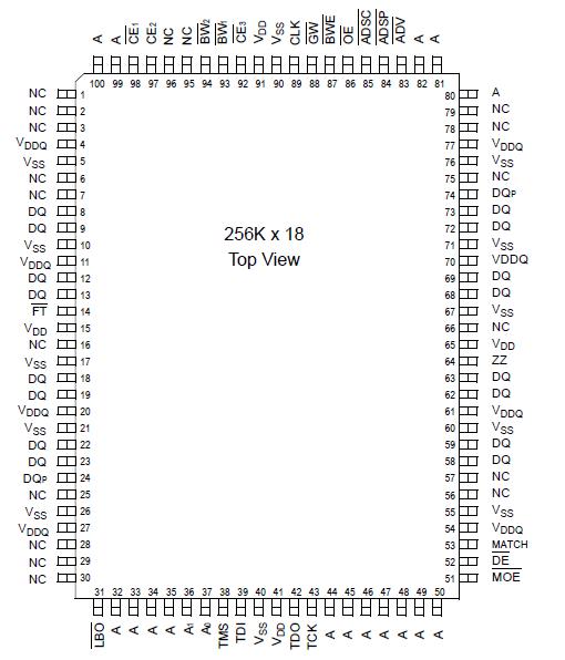 Specifications
| Symbol |
Description |
Value |
Unit |
| VDD |
Voltage on VDD Pins |
0.5 to 4.6 |
V |
| VDDQ |
Voltage in VDDQPins |
0.5 to VDD |
V |
| VCK |
Voltage on Clock Input Pin |
0.5 to 6 |
V |
| VI/O |
Voltage on I/O Pins |
0.5 to VDDQ+0.5 ( 4.6 V max.) |
V |
| VIN |
Voltage on Other Input Pins |
0.5 to VDD +0.5 ( 4.6 V max.) |
V |
| IIN |
Input Current on Any Pin |
+/20 |
mA |
| IOUT |
Output Current on Any I/O Pin |
+/20 |
mA |
| PD |
Package Power Dissipation |
1.5 |
W |
| TSTG |
Storage Temperature |
55 to 125 |
|
| TBIAS |
Temperature Under Bias |
55 to 125 |
|
Note:
Permanent damage to the device may occur if the Absolute Maximun Ratings are exceeded. Functional operation should be restricted to the recommended operation conditions. Exposure to higher than recommended voltages, for an extended period of time, could effect the performance and reliability of this component.DescriptionThe GS84118A is a 256K x 18 high performance synchronous SRAM with integrated Tag RAM comparator. A 2-bit burst counter is included to provide burst interface with Pentium
TM and other high performance CPUs. GS84118A is designed to be used as a Cache Tag SRAM, as well as data SRAM. Addresses, data IOs, match output, chip enables (
CE1, CE2,
CE3), address control inputs (
ADSP,
ADSC,
ADV), and write control inputs (
BW1,
BW2,
BWE,
GW,
DE) are synchronous and are controlled by a positive-edge-triggered clock (CLK).
Output Enable (
OE), Match Output Enable, and power down control (ZZ)of GS84118A are asynchronous. Burst can be initiated with either
ADSP or
ADSC inputs. Subsequent burst addresses are generated internally and are controlled by
ADV. The burst sequence is either interleave order (Pentium
TM or x86) or linear order, and is controlled by
LBO.
Output registers and the Match output register are provided and controlled by the
FT mode pin (Pin 14). Through use of the
FT mode pin, I/O registers can be programmed to perform pipeline or flow through operation. Flow Through mode reduces latency.
Byte write operation of GS84118A is performed by using Byte Write Enable (
BWE) input combined with two individual byte write signals
BW1-2. In addition, Global Write (
GW) is available for writing all bytes at one time.
Compare cycles begin as a read cycle with output disabled so that compare data can be loaded into the data input register. The comparator compares the read data with the registered input data and a match signal is generated. The match output of GS84118A can be either in Pipeline or Flow Through modes controlled by the
FT signal.
Low power (Standby mode)of GS84118A is attained through the assertion of the ZZ signal, or by stopping the clock (CLK). Memory data is retained during Standby mode.
JTAG boundary scan interface of GS84118A is provided using IEEE standard 1149.1 protocol. Four pins-Test Data In (TDI), Test Data Out (TDO), Test Clock (TCK) and Test Mode Select (TMS)-are used to perform JTAG function.
The GS84118A operates on a 3.3 V power supply and all inputs/outputs are 3.3 V or 2.5 V LVTTL-compatible. Separate output (V
DDQ) pins are used to allow both 3.3 V or 2.5 V IO interface.
* Pentium is a trademark of Intel Corp.

 GS84118AT Data Sheet