Output Type
:
Packaging
: Reel
Number of Circuits
: 1
Maximum Operating Temperature
: + 125 C
Package / Case
: SO-16
Minimum Operating Temperature
: - 55 C
Logic Type
: CMOS
Counter Type
: Binary
Number of Input Lines
: 4
Counting Sequence
: Up/Down
Logic Family
: 4029
Propagation Delay Time
: 500 ns, 240 ns, 180 ns
Features: ·MEDIUM SPEED OPERATION : 8MHz (Typ.) at CL = 50pF and VDD - VSS = 10V
·MULTI-PACKAGE PARALLEL CLOCKING FOR SYNCHRONOUS HIGH SPEED OUTPUT RESPONSE OR RIPPLE CLOCKING FOR SLOW CLOCK INPUT RISE AND FALL TIMES
·"PRESET ENABLE" AND INDIVIDUAL "JAM" INPUTS PROVIDED
·BINARY OR DECADE UP/DOWN COUNTING
·BCD OUTPUTS IN DECADE MODE
·QUIESCENT CURRENT SPECIF. UP TO 20V
·STANDARDIZED SYMMETRICAL OUTPUT CHARACTERISTICS
·INPUT LEAKAGE CURRENT
·II = 100nA (MAX) AT VDD = 18V TA = 25°C
·100% TESTED FOR QUIESCENT CURRENT
·MEETS ALL REQUIREMENTS OF JEDEC JESD13B "STANDARD SPECIFICATIONS FOR DESCRIPTION OF B SERIES CMOS DEVICES"Pinout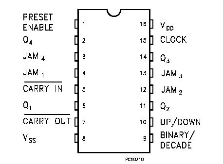 Specifications
|
Symbol |
Rating |
Value |
Unit |
|
VDD |
Supply Voltage |
0.5 to + 22 |
V
|
|
Vi |
DC Input Voltage |
0.5 to VDD + 0.5 |
V |
|
II |
DC Input Current |
± 10 |
mA |
|
PD
|
Power Dissipation per package
Power Dissipation per Output Transistor |
200
100 |
mW
mW |
|
Top |
Operating Temperature |
-55 to +125 |
°C |
|
|
Storage Temperature |
65 to + 150 |
°C |
Absolute Maximum Ratings are those values beyond which damage to the device may occur. Functional operation under these conditions is
not implied.
All voltage values are referred to VSS pin voltage.DescriptionHCF4029B is a monolithic integrated circuit fabricated in Metal Oxide Semiconductor technology available in DIP and SOP packages. HCF4029B consists of a four stage binary or BCD-decade up/down counter with provisions for look ahead carry in both counting modes. The inputs consist of a single CLOCK, CARRY IN (CLOCK ENABLE) , BINARY/DECADE, UP/ DOWN, PRESET ENABLE, and four individual JAM signals. Q1, Q2, Q3, Q4 and a CARRY OUT signal are provided as outputs. A high PRESET ENABLE signal allows information on the JAM INPUTS to preset the counter to any state asynchronously with the clock. A low on each JAM line, when the PRESET-ENABLE signal is high, resets the counter to its zero count. The counter advances one count at the positive transition of the clock when the CARRY-IN and PRESET ENABLE signals are low. Advancement is inhibited when the CARRY-IN or PRESET ENABLE signals are high. The CARRY-OUT

 HCF4029M013TR Data Sheet