HCF4097B

Features: `LOW ON RESISTANCE: 125W (typ.) OVER 15 Vp-p SIGNAL INPUT RANGE FOR VDD - VSS = 15V`HIGH OFF RESISTANCE: CHANNEL LEAKAGE OF ±10pA (typ.) @ VDD - VSS = 10V `MATCHED SWITCH CHARACTERISTICS: DRON = 5W(typ.) FOR VDD - VSS = 15V`VERY LOW QUIESCENT POWER DISSIPATION UNDER A DIGITAL CONTROL INP...

product image

HCF4097B Picture
SeekIC No. : 004359700 Detail

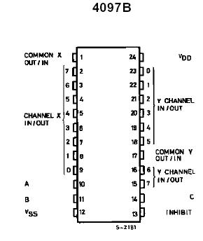
HCF4097B: Features: `LOW ON RESISTANCE: 125W (typ.) OVER 15 Vp-p SIGNAL INPUT RANGE FOR VDD - VSS = 15V`HIGH OFF RESISTANCE: CHANNEL LEAKAGE OF ±10pA (typ.) @ VDD - VSS = 10V `MATCHED SWITCH CHARACTERISTICS: ...

floor Price/Ceiling Price
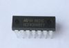
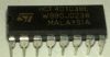
Part Number:
HCF4097B
Supply Ability:
5000

Price Break

  • Qty
  • 1~5000
  • Unit Price
  • Negotiable
  • Processing time
  • 15 Days
Total Cost: $ 0.00

SeekIC Buyer Protection PLUS - newly updated for 2013!

  • Escrow Protection.
  • Guaranteed refunds.
  • Secure payments.
  • Learn more >>

Month Sales

268 Transactions

Rating

evaluate  (4.8 stars)

Upload time: 2024/5/5

Payment Methods

All payment methods are secure and covered by SeekIC Buyer Protection PLUS.

Notice: When you place an order, your payment is made to SeekIC and not to your seller. SeekIC only pays the seller after confirming you have received your order. We will also never share your payment details with your seller.
Product Details

Description


Features:

`LOW ON RESISTANCE: 125W (typ.) OVER 15 Vp-p SIGNAL INPUT RANGE FOR VDD - VSS = 15V
`HIGH OFF RESISTANCE: CHANNEL LEAKAGE OF ±10pA (typ.) @ VDD - VSS = 10V
`MATCHED SWITCH CHARACTERISTICS: DRON = 5W(typ.) FOR VDD - VSS = 15V
`VERY LOW QUIESCENT POWER DISSIPATION UNDER A DIGITAL CONTROL INPUT AND SUPPLY CONDITIONS: 0.2mW (typ.) @ VDD -VSS = 10V
`BINARY ADDRESSDECODING ON CHIP
`QUIESCENT CURRENT SPECIFIED TO 20V FOR HCC DEVICE
`STANDARDIZED SYMMETRICAL OUTPUT CHARACTERISTICS
`5V, 10V AND 15V PARAMETRIC RATINGS
`INPUT CURRENT OF 100nA AT 18V AND25 FOR HCC DEVICE
`100% TESTEDFOR QUIESCENT CURRENT
`MEETSALLREQUIREMENTSOFJEDECTENTATIVE STANDARD No 13A, "STANDARD SPECIFICATIONS FOR DESCRIPTION OF B SERIE CMOS DEVICES"


Pinout

  Connection Diagram


Specifications

Symbol Parameter Value Unit
VDD* Supply Voltage :HCC Types
HCF Types
0.5 to + 20
0.5 to + 18
V
V
Vi Input Voltage 0.5 to VDD + 0.5 V
II DC Input Current (any one input) ± 10 mA
Ptot Total Power Dissipation (per package)
Dissipation per Output Transistor
for Top = Full Package-temperature Range
200
100
mW
mW
Top Operating Temperature : HCC Types
HCF Types
55 to + 125
40 to + 85

Tstg Storage Temperature 65 to + 150


Description

In the HCC/HCF4067B and HCC/HCF4097B  series, the HCC4067B, HCC4097B (extended temperature range) and HCF4067B, HCF4097B (intermediate temperature range) are monolithic integrated circuits available in 24-lead dual in line plastic or ceramic package.

The HCC/HCF4067B and HCC/HCF4097B COS/MOS analog multiplexers/demultiplexers are digitally controlled analog switches having low ON impedance, low OFF leakage current and internal address decoding. in addition, the ON resistance is relatively constant over the full input-signal range. The HCC/HCF4067B ia a 16-channel multiplexer with four binary control inputs A, B, C, D, and an inhibit input, arranged so that any combination of the inputs selects one switch.The HCC/HCF4097 is a differential 8-channel multiplexerhaving three binary control inputs A, B, C, and an inhibit input. The inputs permit selection of one


Customers Who Bought This Item Also Bought

Margin,quality,low-cost products with low minimum orders. Secure your online payments with SeekIC Buyer Protection.
Undefined Category
Test Equipment
Boxes, Enclosures, Racks
Industrial Controls, Meters
Potentiometers, Variable Resistors
View more