HD64F3048

Features: Upward-compatible with the H8/300 CPU at the object-code levelGeneral-register machine• Sixteen 16-bit general registers(also usable as + eight 16-bit registers or eight 32-bit registers)High-speed operation (flash memory version)• Maximum clock rate: 16 MHz• Add/subtra...

product image

HD64F3048 Picture
SeekIC No. : 004360313 Detail

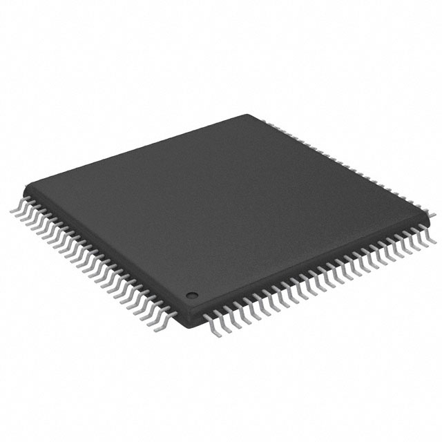
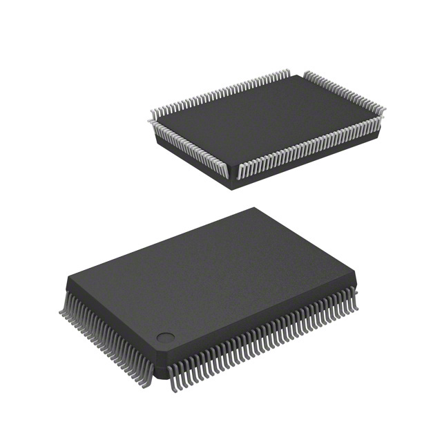
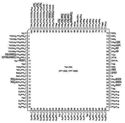
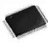
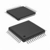
HD64F3048: Features: Upward-compatible with the H8/300 CPU at the object-code levelGeneral-register machine• Sixteen 16-bit general registers(also usable as + eight 16-bit registers or eight 32-bit regis...

floor Price/Ceiling Price

Part Number:
HD64F3048
Supply Ability:
5000

Price Break

  • Qty
  • 1~5000
  • Unit Price
  • Negotiable
  • Processing time
  • 15 Days
Total Cost: $ 0.00

SeekIC Buyer Protection PLUS - newly updated for 2013!

  • Escrow Protection.
  • Guaranteed refunds.
  • Secure payments.
  • Learn more >>

Month Sales

268 Transactions

Rating

evaluate  (4.8 stars)

Upload time: 2024/4/28

Payment Methods

All payment methods are secure and covered by SeekIC Buyer Protection PLUS.

Notice: When you place an order, your payment is made to SeekIC and not to your seller. SeekIC only pays the seller after confirming you have received your order. We will also never share your payment details with your seller.
Product Details

Description


Features:

Upward-compatible with the H8/300 CPU at the object-code level
General-register machine
• Sixteen 16-bit general registers
(also usable as + eight 16-bit registers or eight 32-bit registers)
High-speed operation (flash memory version)
• Maximum clock rate: 16 MHz
• Add/subtract: 125 ns
• Multiply/divide: 875 ns
High-speed operation (masked ROM and PROM versions)
• Maximum clock rate: 18 MHz
• Add/subtract: 111 ns
• Multiply/divide: 778 ns
16-Mbyte address space
Instruction features
• 8/16/32-bit data transfer, arithmetic, and logic instructions
• Signed and unsigned multiply instructions (8 bits × 8 bits, 16 bits × 16 bits)
• Signed and unsigned divide instructions (16 bits ÷ 8 bits, 32 bits ÷ 16 bits)
• Bit accumulator function
• Bit manipulation instructions with register-indirect specification of bit positions
H8/3048
• ROM: 128 kbytes
• RAM: 4 kbytes
H8/3047
• ROM: 96 kbytes
• RAM: 4 kbytes
H8/3045
• ROM: 64 kbytes
• RAM: 2 kbytes
H8/3044
• ROM: 32 kbytes
• RAM: 2 kbytes
• Seven external interrupt pins: NMI, IRQ0 to IRQ5
• 30 internal interrupts
• Three selectable interrupt priority levels
• Address space can be partitioned into eight areas, with independent bus specifications in each area
• Chip select output available for areas 0 to 7
• 8-bit access or 16-bit access selectable for each area
• Two-state or three-state access selectable for each area
• Selection of four wait modes
• Bus arbitration function
DRAM refresh
controller
• Directly connectable to 16-bit-wide DRAM
• CAS-before-RAS refresh
• Self-refresh mode selectable
Pseudo-static RAM refresh
• Self-refresh mode selectable
Short address mode
• Maximum four channels available
• Selection of I/O mode, idle mode, or repeat mode
• Can be activated by compare match/input capture A interrupts from ITU
channels 0 to 3, transmit-data-empty and receive-data-full interrupts from SCI
channel 0, or external requests
Full address mode
• Maximum two channels available
• Selection of normal mode or block transfer mode
• Can be activated by compare match/input capture A interrupts from ITU
channels 0 to 3, external requests, or auto-request

Usable as an interval timer
• Five 16-bit timer channels, capable of processing up to 12 pulse outputs or 10 pulse inputs
• 16-bit timer counter (channels 0 to 4)
• Two multiplexed output compare/input capture pins (channels 0 to 4)
• Operation can be synchronized (channels 0 to 4)
• PWM mode available (channels 0 to 4)
• Phase counting mode available (channel 2)
• Buffering available (channels 3 and 4)
• Reset-synchronized PWM mode available (channels 3 and 4)
• Complementary PWM mode available (channels 3 and 4)
• DMAC can be activated by compare match/input capture A interrupts (channels 0 to 3)


Pinout

  Connection Diagram


Specifications

Item
Symbol
Value
Unit
Power supply voltage  
VCC
0.3 to +7.0
V
Programming voltage HD6473048
VPP
0.3 to +13.5
V
HD64F3048
0.3 to +13.0
V
Input voltage (except for MD2 and port 7  
Vin
0.3 to VCC + 0.3
V
Input voltage (MD2) HD6473048,
HD6433048,
HD6433047,
HD6433045,
HD6433044
Vin
0.3 to VCC + 0.3
V
HD64F3048
0.3 to +13.0
V
Input voltage (port 7)
Vin
0.3 to AVCC + 0.3
V
Reference voltage
VREF
0.3 to AVCC + 0.3
V
Analog power supply voltage
AVCC
0.3 to +7.0
V
Analog input voltage
VAN
0.3 to AVCC + 0.3
V
Operating temperature
Topr
Regular specifications: 20 to +75
°C
Wide-range specifications: 40 to +85
°C
Storage temperature
Tstg
55 to +125
°C
Caution: Permanent damage to the chip may result if absolute maximum ratings are exceeded.Particularly, insure that peak overshoot at the VPP and MD2 pins does not exceed 13 V.


Customers Who Bought This Item Also Bought

Margin,quality,low-cost products with low minimum orders. Secure your online payments with SeekIC Buyer Protection.
Audio Products
Integrated Circuits (ICs)
Transformers
Fans, Thermal Management
View more