HD74CDC857

Features: * Supports 100 MHz to 150 MHz operation range *1* Distributes one differential clock input pair to ten differential clock outputs pairs* SSTL_2 (Stub Series Terminated Logic) differential inputs and LVCMOS reset (G) input* Supports spread spectrum clock* External feedback pins (FBIN, FBI...

product image

HD74CDC857 Picture
SeekIC No. : 004360601 Detail

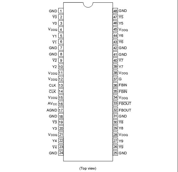
HD74CDC857: Features: * Supports 100 MHz to 150 MHz operation range *1* Distributes one differential clock input pair to ten differential clock outputs pairs* SSTL_2 (Stub Series Terminated Logic) differential ...
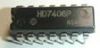
floor Price/Ceiling Price

Part Number:
HD74CDC857
Supply Ability:
5000

Price Break

  • Qty
  • 1~5000
  • Unit Price
  • Negotiable
  • Processing time
  • 15 Days
Total Cost: $ 0.00

SeekIC Buyer Protection PLUS - newly updated for 2013!

  • Escrow Protection.
  • Guaranteed refunds.
  • Secure payments.
  • Learn more >>

Month Sales

268 Transactions

Rating

evaluate  (4.8 stars)

Upload time: 2024/4/24

Payment Methods

All payment methods are secure and covered by SeekIC Buyer Protection PLUS.

Notice: When you place an order, your payment is made to SeekIC and not to your seller. SeekIC only pays the seller after confirming you have received your order. We will also never share your payment details with your seller.
Product Details

Description


Features:

*  Supports 100 MHz to 150 MHz operation range *1
*  Distributes one differential clock input pair to ten differential clock outputs pairs
*  SSTL_2 (Stub Series Terminated Logic) differential inputs and LVCMOS reset (G) input
*  Supports spread spectrum clock
*  External feedback pins (FBIN, FBIN) are used to synchronize the outputs to the clock input
*  Supports both 3.3 V/2.5V analog supply voltage (AVCC), and 2.5 V VDDQ
*  No external RC network required
*  Sleep mode detection
*  48pin TSSOP (Thin Shrink Small Outline Package)
Note: 1. 200 MHz (Max) ver. will be available by 4Q/'99


Pinout

  Connection Diagram


Specifications

Item

Symbol

Ratings

Unit

Test Conditions

Supply voltage

VCC

0.5 to 4.6

V


Input voltage

VI

0.5 to 4.6

V


Output voltage *1

VO

0.5 to V + 0.50.5 to 4.6

V


Input clamp current

IIK

50

mA

VI < 0

Output clamp current

IOK

-50

mA

VO < 0

Continuous output current

IO

50

mA

VO = 0 to VDDQ

Continuous current through
VDDQ or GND

ICC or IGND

100

mA


Maximum power dissipation

at Ta = 55 C (in still air)

PT

0.7

mW


Storage temperature

Tstg

65 to 150

C


Description

The HD74CDC857 is a high-performance, low-skew, low-jitter, phase locked loop clock driver.  It is specifically designed for use with DDR (Double Data Rate) synchronous DRAMs.


Customers Who Bought This Item Also Bought

Margin,quality,low-cost products with low minimum orders. Secure your online payments with SeekIC Buyer Protection.
Integrated Circuits (ICs)
Discrete Semiconductor Products
Transformers
Soldering, Desoldering, Rework Products
Power Supplies - External/Internal (Off-Board)
View more