HD74LV1G08A

Features: ` The basic gate function is lined up as hitachi uni logic series.` Supplied on emboss taping for high speed automatic mounting.` Electrical characteristics equivalent to the HD74LV08A Supply voltage range : 1.65 to 5.5 V Operating temperature range : 40 to +85°C` All inputs VIH (Max.) =...

product image

HD74LV1G08A Picture
SeekIC No. : 004360713 Detail

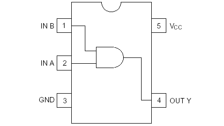
HD74LV1G08A: Features: ` The basic gate function is lined up as hitachi uni logic series.` Supplied on emboss taping for high speed automatic mounting.` Electrical characteristics equivalent to the HD74LV08A Sup...

floor Price/Ceiling Price

Part Number:
HD74LV1G08A
Supply Ability:
5000

Price Break

  • Qty
  • 1~5000
  • Unit Price
  • Negotiable
  • Processing time
  • 15 Days
Total Cost: $ 0.00

SeekIC Buyer Protection PLUS - newly updated for 2013!

  • Escrow Protection.
  • Guaranteed refunds.
  • Secure payments.
  • Learn more >>

Month Sales

268 Transactions

Rating

evaluate  (4.8 stars)

Upload time: 2024/5/1

Payment Methods

All payment methods are secure and covered by SeekIC Buyer Protection PLUS.

Notice: When you place an order, your payment is made to SeekIC and not to your seller. SeekIC only pays the seller after confirming you have received your order. We will also never share your payment details with your seller.
Product Details

Description


Features:

`  The basic gate function is lined up as hitachi uni logic series.
`  Supplied on emboss taping for high speed automatic mounting.
`  Electrical characteristics equivalent to the HD74LV08A
     Supply voltage range : 1.65 to 5.5 V
     Operating temperature range : 40 to +85°C
`  All inputs VIH (Max.) = 5.5 V (@VCC = 0 V to 5.5 V)
     All outputs VO (Max.) = 5.5 V (@VCC = 0 V)
`  Output current ±6 mA (@VCC = 3.0 V to 3.6 V), ±12 mA (@VCC = 4.5 V to 5.5 V)
`  All the logical input has hysteresis voltage for the slow transition.


Pinout

  Connection Diagram


Specifications

Item
Symbol
Ratings
Unit
Test Conditions
Supply voltage range
VCC
0.5 to 7.0
V
V
Input voltage range*1
VI
0.5 to 7.0
V
V
Output voltage range*1, 2
VO
0.5 to VCC + 0.5
V
Output: H or L
0.5 to 7.0
VCC: OFF
Input clamp current
IIK
20
mA
VI < 0
Output clamp current
IOK
±50
mA
VO < 0 or VO > VCC
Continuous output current
IO
±25
mA
VO = 0 to VCC
Continuous current through
VCC or GND
ICC or IGND
±50
mA
Maximum power dissipation
at Ta = 25(in still air)*3
PT
200
mW
 
Storage temperature
Tstg
65 to 150

Notes: The absolute maximum ratings are values which must not individually be exceeded, and furthermore, no two 
            of which may be realized at the same time.

1. The input and output voltage ratings may be exceeded if the input and output clamp-current ratings are observed.
2. This value is limited to 5.5 V maximum.
3. The maximum package power dissipation was calculated using a junction temperature of 150.


Description

The HD74LV1G08A has twoinput AND gate in a 5 pin package. Low voltage and high speed operation is suitable for the battery powered products (e.g., notebook computers), and the low power consumption extends the battery life.


Customers Who Bought This Item Also Bought

Margin,quality,low-cost products with low minimum orders. Secure your online payments with SeekIC Buyer Protection.
Test Equipment
Circuit Protection
Audio Products
View more