HEF4035B

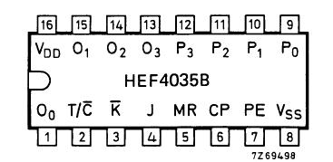
PinoutDescriptionThe HEF4035B is a fully synchronous edge-triggered 4-bit shift register with a clock input (CP), four synchronous parallel data inputs (P0 to P3), two synchronous serial data inputs (J, K), a synchronous parallel enable input (PE), buffered parallel outputs from all 4-bit position...

product image

HEF4035B Picture
SeekIC No. : 004361351 Detail

HEF4035B: PinoutDescriptionThe HEF4035B is a fully synchronous edge-triggered 4-bit shift register with a clock input (CP), four synchronous parallel data inputs (P0 to P3), two synchronous serial data inputs...

floor Price/Ceiling Price

Part Number:
HEF4035B
Supply Ability:
5000

Price Break

  • Qty
  • 1~5000
  • Unit Price
  • Negotiable
  • Processing time
  • 15 Days
Total Cost: $ 0.00

SeekIC Buyer Protection PLUS - newly updated for 2013!

  • Escrow Protection.
  • Guaranteed refunds.
  • Secure payments.
  • Learn more >>

Month Sales

268 Transactions

Rating

evaluate  (4.8 stars)

Upload time: 2024/4/30

Payment Methods

All payment methods are secure and covered by SeekIC Buyer Protection PLUS.

Notice: When you place an order, your payment is made to SeekIC and not to your seller. SeekIC only pays the seller after confirming you have received your order. We will also never share your payment details with your seller.
Product Details

Description


Pinout

  Connection Diagram


Description

The HEF4035B is a fully synchronous edge-triggered 4-bit shift register with a clock input (CP), four synchronous parallel data inputs (P0 to P3), two synchronous serial data inputs (J, K), a synchronous parallel enable input (PE), buffered parallel outputs from all 4-bit positions (O0 to O3), a true/complement input (T/C) and an overriding asynchronous master reset input (MR). Each HEF4035B register is of a D-type master-slave flip-flop. Operation is synchronous (except for MR) and is edge-triggered on the LOW to HIGH transition of the CP input. When PE is HIGH, data is loaded into the register from P0 to P3 on the LOW to HIGH transition of CP.

When PE of HEF4035B  is LOW, data is shifted into the first register position from J and K and all the data in the register is shifted one position to the right on the LOW to HIGH transition of CP. D-type entry is obtained by interconnecting J and K. When J = HIGH and K = LOW the first stage is in the toggle mode.

When J = LOW and K = HIGH the first stage is in the hold mode. The outputs (O0 to O3) of HEF4035B are either inverting or non-inverting, depending on T/C state. With T/C HIGH, O0 to O3 are non-inverting (active HIGH) and when T/C is LOW, O0 to O3 are inverting (active LOW). A HIGH on MR resets all four bit positions (O0 to O3 = LOW if T/C = HIGH, O0 to O3 = HIGH if T/C = LOW) independent of all other input conditions. Schmitt-trigger action in the clock input makes the circuit highly tolerant to slower clock rise and fall times.


Customers Who Bought This Item Also Bought

Margin,quality,low-cost products with low minimum orders. Secure your online payments with SeekIC Buyer Protection.
Cables, Wires - Management
Crystals and Oscillators
Optical Inspection Equipment
Soldering, Desoldering, Rework Products
Hardware, Fasteners, Accessories
Discrete Semiconductor Products
View more