HEF4051BP

DescriptionThe HEF4051BP is designed as an 8-channel analogue multiplexer /demultiplexer with three address inputs (A0 to A2), an active LOW enable input (E), eight independent inputs/outputs (Y0 to Y7) and a common input/output (Z). HEF4051BP contains eight bidirectional analogue switches, each w...

product image

HEF4051BP Picture
SeekIC No. : 004361365 Detail

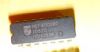
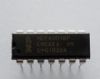
HEF4051BP: DescriptionThe HEF4051BP is designed as an 8-channel analogue multiplexer /demultiplexer with three address inputs (A0 to A2), an active LOW enable input (E), eight independent inputs/outputs (Y0 to...

floor Price/Ceiling Price

Part Number:
HEF4051BP
Supply Ability:
5000

Price Break

  • Qty
  • 1~5000
  • Unit Price
  • Negotiable
  • Processing time
  • 15 Days
Total Cost: $ 0.00

SeekIC Buyer Protection PLUS - newly updated for 2013!

  • Escrow Protection.
  • Guaranteed refunds.
  • Secure payments.
  • Learn more >>

Month Sales

268 Transactions

Rating

evaluate  (4.8 stars)

Upload time: 2024/4/30

Payment Methods

All payment methods are secure and covered by SeekIC Buyer Protection PLUS.

Notice: When you place an order, your payment is made to SeekIC and not to your seller. SeekIC only pays the seller after confirming you have received your order. We will also never share your payment details with your seller.
Product Details

Description


Description

The HEF4051BP is designed as an 8-channel analogue multiplexer /demultiplexer with three address inputs (A0 to A2), an active LOW enable input (E), eight independent inputs/outputs (Y0 to Y7) and a common input/output (Z). HEF4051BP contains eight bidirectional analogue switches, each with one side connected to an independent input/output (Y0 to Y7) and the other side connected to a common input/output (Z).

Some limiting ratings of HEF4051BP has been concluded as follow. Its supply voltage with reference to Vdd would be from -18V to +0.5V. To avoid drawing Vdd current out of terminal Z, when switch current flows into terminals Y, the voltage drop across the bidirectional switch must not exceed 0,4V. If the switch current flows into terminal Z, no Vdd current will flow out of terminals Y, in this case there is no limit for the voltage drop across the switch, but the voltages at Y and Z may not exceed Vdd or Vee.

Also some electrical characteristics of HEF4051BP are concluded as follow. (1)Its ON resistance with test conditios of Vis=0 to Vdd-Vee would be typ 350 and max 2500 at Vdd-Vee=5V and would be typ 80 and max 245 at 10V and would be typ 60 and max 175 at 15V. (2)Its ON resistance with conditions of Vis=0 would be typ 115 and max 340 at Vdd-Vee=5V and would be typ 50 and max 160 at 10V and would be typ 40 and max 115 at 15V. (3)Its ON resistance with test conditions of Vis=Vdd-Vee would be typ 120 and max 365 at Vdd-Vee=5V and would be typ 65 and max 200 at 10V and would be typ 50 and max 155 at 15V. (4)Its off-state leakage current all channels off would be max 100nA at Vdd-Vee=15V. (5)Its off-state leakage current any channel would be max 200nA at Vdd-Vee=15V.  (6)Its propagation delays Vis to Vos high to low would be typ 15ns and max 30ns at Vdd=5V and would be typ 5ns and max 10ns at Vdd=10V and would be typ 5ns and max 10ns at Vdd=15V. (7)Its propagation delays Vis to Vos low to high would be typ 15ns and max 30ns at Vdd=5V and would be typ 5ns and max 10ns at Vdd=10V and would be typ 5ns and max 10ns at Vdd=15V. And so on. If you have any question or suggestion or want to know more information of HEF4051BP,  please contact us for details. Thank you!


Customers Who Bought This Item Also Bought

Margin,quality,low-cost products with low minimum orders. Secure your online payments with SeekIC Buyer Protection.
Semiconductor Modules
Discrete Semiconductor Products
Connectors, Interconnects
RF and RFID
Power Supplies - Board Mount
View more