HEF4104B

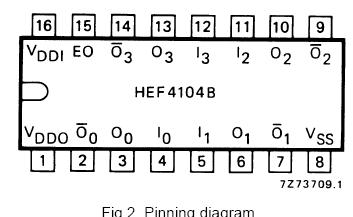
PinoutDescriptionThe HEF4104B quadruple low voltage to high voltage translator with 3-state outputs provides the capability of interfacing low voltage circuits to high voltage circuits, such as low voltage LOCMOS and TTL to high voltage LOCMOS. HEF4104B has four data inputs (I0 to I3), an active H...

product image

HEF4104B Picture
SeekIC No. : 004361395 Detail

HEF4104B: PinoutDescriptionThe HEF4104B quadruple low voltage to high voltage translator with 3-state outputs provides the capability of interfacing low voltage circuits to high voltage circuits, such as low ...

floor Price/Ceiling Price

Part Number:
HEF4104B
Supply Ability:
5000

Price Break

  • Qty
  • 1~5000
  • Unit Price
  • Negotiable
  • Processing time
  • 15 Days
Total Cost: $ 0.00

SeekIC Buyer Protection PLUS - newly updated for 2013!

  • Escrow Protection.
  • Guaranteed refunds.
  • Secure payments.
  • Learn more >>

Month Sales

268 Transactions

Rating

evaluate  (4.8 stars)

Upload time: 2024/4/29

Payment Methods

All payment methods are secure and covered by SeekIC Buyer Protection PLUS.

Notice: When you place an order, your payment is made to SeekIC and not to your seller. SeekIC only pays the seller after confirming you have received your order. We will also never share your payment details with your seller.
Product Details

Description


Pinout

  Connection Diagram


Description

The HEF4104B quadruple low voltage to high voltage translator with 3-state outputs provides the capability of interfacing low voltage circuits to high voltage circuits, such as low voltage LOCMOS and TTL to high voltage LOCMOS. HEF4104B has four data inputs (I0 to I3), an active HIGH output enable input (EO), four data outputs (O0 to O3) and their complements (O0 to O3).

With EO HIGH, O0 to O3 and O0 to O3 are in the low impedance ON-state, either HIGH or LOW as determined by I0 to I3; with EO LOW, O0 to O3 and O0 to O3 are in the high impedance OFF-state. The HEF4104B uses a common negative supply (VSS) and separate positive supplies for inputs (VDDI) and outputs (VDD0). VDDI must always be less than or equal to VDDO, even during power turn-on and turn-off. For the permissible operating range of VDDI and VDDO see graph Fig.4.

Each input protection circuit of HEF4104B is terminated between VDDO and VSS. This allows the input signals to be driven from any potential between VDDO and VSS, without regard to current limiting. When driving from potentials greater than VDDO or less than VSS, the current at each input must be limited to 10 mA.


Customers Who Bought This Item Also Bought

Margin,quality,low-cost products with low minimum orders. Secure your online payments with SeekIC Buyer Protection.
Static Control, ESD, Clean Room Products
Tapes, Adhesives
803
Line Protection, Backups
Semiconductor Modules
Sensors, Transducers
Transformers
View more