HG74ALVC16835C

Features: · Ideal for Use in PC100 Registered DIMM· 0.5mm CMOS Technology· 2.3 ~ 3.6 VCC Operation· Balanced Output Drive(±24mA)· Package Options Include Plastic Thin Shrink Small-Outline Packages, Shrink Small-Outline Packages (TSSOP 56 Pins, SSOP 56 Pins, TVSOP56 Pins)PinoutSpecifications S...

product image

HG74ALVC16835C Picture
SeekIC No. : 004362082 Detail

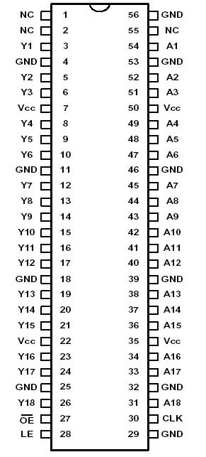
HG74ALVC16835C: Features: · Ideal for Use in PC100 Registered DIMM· 0.5mm CMOS Technology· 2.3 ~ 3.6 VCC Operation· Balanced Output Drive(±24mA)· Package Options Include Plastic Thin Shrink Small-Outline Packages, ...

floor Price/Ceiling Price

Part Number:
HG74ALVC16835C
Supply Ability:
5000

Price Break

  • Qty
  • 1~5000
  • Unit Price
  • Negotiable
  • Processing time
  • 15 Days
Total Cost: $ 0.00

SeekIC Buyer Protection PLUS - newly updated for 2013!

  • Escrow Protection.
  • Guaranteed refunds.
  • Secure payments.
  • Learn more >>

Month Sales

268 Transactions

Rating

evaluate  (4.8 stars)

Upload time: 2024/4/25

Payment Methods

All payment methods are secure and covered by SeekIC Buyer Protection PLUS.

Notice: When you place an order, your payment is made to SeekIC and not to your seller. SeekIC only pays the seller after confirming you have received your order. We will also never share your payment details with your seller.
Product Details

Description


Features:

· Ideal for Use in PC100 Registered DIMM
· 0.5mm CMOS Technology
· 2.3 ~ 3.6 VCC Operation
· Balanced Output Drive(±24mA)
· Package Options Include Plastic Thin Shrink Small-Outline Packages, Shrink Small-Outline Packages (TSSOP 56 Pins, SSOP 56 Pins, TVSOP56 Pins)


Pinout

  Connection Diagram


Specifications

Symbols Parameter Value Conditions
VCC Supply Voltage Range -0.5 V to 4.6 V  
VI Input Voltage Range (see note 1) -0.5 V to VCC + 0.5 V  
VO Output Voltage Range (see notes 1 and 2) -0.5 V to VCC + 0.5 V  
IIK Input Clamp Current -50 mA VI < 0
IOK Output Clamp Current ±50 mA VO <0 or VO >VCC
IO Continuous Output Current ±50 mA VO =0 to VCC
ICC Continuous Current through each VCC +100 mA  
IGND Continuous Current through each GND -100 mA  
Tstg Storage Temperature Range - 65°C to 150°C  


Description

The HG74ALVC16835C is an 18-bit universal bus driver designed for 2.3V to 3.6 V VCC Operation.

The Output-Enable(OE ) controls data flow from A to Y. The HG74ALVC16835C operates in transparent mode when the latch-enable(LE) input is high. When LE is low, the A data is latched if the clock input is held at a high or low logic level.If LE is low, the A data is stored in the latch/flip-flop on the low-to-high transition of CLK.When OE is high, the Outputs are in the high impedance state. OE should be tied to VCC through a pull up resistor to ensure the high impedance state during power up or power down.

The HG74ALVC16835C is characterized for operation from -40°C to 85°C.


Customers Who Bought This Item Also Bought

Margin,quality,low-cost products with low minimum orders. Secure your online payments with SeekIC Buyer Protection.
Tapes, Adhesives
803
Crystals and Oscillators
Static Control, ESD, Clean Room Products
Line Protection, Backups
Boxes, Enclosures, Racks
Power Supplies - External/Internal (Off-Board)
View more