HT82V842

Features: ` Operating voltage: 2.7V~3.6V` Low power consumption: 70mW (Typ.)` Power down mode: less than 30W` Accepts a direct signal input to ADC or PGA at 1.0 VPP (Typ.)` CCD signal input level: 1.1 VP-P (Max.)` 10-bit ADC (up to 20MHz)- DNL: ±0.6 LSB (Typ.)` Black level neutralizer, target sett...

product image

HT82V842 Picture
SeekIC No. : 004367114 Detail

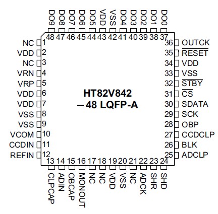
HT82V842: Features: ` Operating voltage: 2.7V~3.6V` Low power consumption: 70mW (Typ.)` Power down mode: less than 30W` Accepts a direct signal input to ADC or PGA at 1.0 VPP (Typ.)` CCD signal input level: 1...

floor Price/Ceiling Price

Part Number:
HT82V842
Supply Ability:
5000

Price Break

  • Qty
  • 1~5000
  • Unit Price
  • Negotiable
  • Processing time
  • 15 Days
Total Cost: $ 0.00

SeekIC Buyer Protection PLUS - newly updated for 2013!

  • Escrow Protection.
  • Guaranteed refunds.
  • Secure payments.
  • Learn more >>

Month Sales

268 Transactions

Rating

evaluate  (4.8 stars)

Upload time: 2024/4/23

Payment Methods

All payment methods are secure and covered by SeekIC Buyer Protection PLUS.

Notice: When you place an order, your payment is made to SeekIC and not to your seller. SeekIC only pays the seller after confirming you have received your order. We will also never share your payment details with your seller.
Product Details

Description


Features:

` Operating voltage: 2.7V~3.6V
` Low power consumption: 70mW (Typ.)
` Power down mode: less than 30W
` Accepts a direct signal input to ADC or PGA at 1.0 VPP (Typ.)
` CCD signal input level: 1.1 VP-P (Max.)
` 10-bit ADC (up to 20MHz)
- DNL: ±0.6 LSB (Typ.)
` Black level neutralizer, target setting: 16~127LSB
` Built-in serial interface
` Independent ADC input conversion clock and data output clock
` Independent CDS and PGA gain control
-  CDS: -1.94/0/6/12dB
- PGA: 0~24dB
` Wide gain range: -1.94~36dB
` High speed sample and hold circuit: pulse width 11ns (Min.)
` 48-pin LQFP package


Pinout

  Connection Diagram


Specifications

Supply Voltage .........................GND-0.3V to GND+6V
Input Voltage .......................... VSS-0.3V to VDD+0.3V
Storage Temperature ..........................-55 to 150
Operating Temperature .........................-20 to 70

Note: These are stress ratings only. Stresses exceeding the range specified under "Absolute Maximum Ratings" may cause substantial damage to the device. Functional operation of this device at other conditions beyond those listed in the specification is not implied and prolonged exposure to extreme conditions may affect device reliability.


Description

The HT82V842 is a CMOS single-chip signal processing device for CCD area sensors. It consists of a clamp circuit, Correlated Double Sampler (CDS), Programmable Gain Amplifier (PGA), reference voltage generator, black level detection circuit, 20MHz 10-bit A/D converter (ADC), timing generator for internally required pulses, serial interface for internal function control and PGA gain control.


Customers Who Bought This Item Also Bought

Margin,quality,low-cost products with low minimum orders. Secure your online payments with SeekIC Buyer Protection.
Boxes, Enclosures, Racks
Circuit Protection
Optoelectronics
Potentiometers, Variable Resistors
Cables, Wires
Fans, Thermal Management
View more