Features: · Processed with HVDI technology
· Symmetric row drive
· Output voltage up to 275V
· Source/Sink current 300mA (min.)
· Shift Register Speed 3MHz
· Pin-programmable shift direction (DIR)
· Hi-Rel processing availablePinout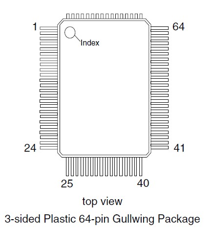 Specifications
Logic supply voltage, LVDD1 -0.5V to +15V
Output supply voltage, VDD1 -0.5V to +15V
Substrate bias voltage, Vsub See Note 3
Output voltage, HVOUT ±300V
Logic input levels -0.5V to VDD +0.5V
Continuous total power dissipation2 Ceramic 1900mW
Plastic 1200mW
Operating temperature range Plastic -40 to +85
Ceramic -55 to +125
Storage temperature range -65 to +150
Lead temperature 1.6mm (1/16 inch) 260
from case for 10 seconds
Notes:
1. All voltages are referenced to VSS.
2. For operation above 25°C ambient derate linearly to maximum operating temperture at 20mW/°C for plasitc and at 19mW/°C for ceramic.
3. Vsub must be the most positive with respect to VSS.
DescriptionThe HV506 is a low-voltage serial to high-voltage parallel converter with push-pull outputs. It is especially suitable for use as a symmetric row driver in AC thin-film electroluminescent (ACTFEL) displays.
There are some features about HV506:When the data reset pin (DRIO) is at logic high, HV506 will reset all the outputs of the internal shift register to zero. At the same time, the output of the shift register will start shifting a logic high from the least significant bit to the most significant bit. The DRIO can be triggered at any time. The DIR pin controls the direction of data through the device. When DIR is at logic high, DRIOA is the input and DRIOB is the output. When DIR is grounded, DRIOB is the input and the DRIOA is the output. See the Output Sequence Operation Table for output sequence. The POL and OE pins perform the polarity select and output enable function respectively. Data is clocked through the shift register loaded on the low to high transition of the clock. A logic high in the shift register will cause the other corresponding output to swing to VDD if POL is high, or to VSS if POL is low. All other outputs will be in the High-Z state. If OE is at logic high all outputs will be in the High-Z state. An output in the High-Z state may block up to 275V above VSS or 275V below VDD. The DP/DN pins are for the positive/negative discharge of the high voltage output HVOUT. Data output buffers are provided for cascading devices.
LVDD requires low current for the HV506 logic section. VDD requires high current for the output section . Typically these two pins are at the same potential. The same current and potential conditions apply to the LVSS, logic, and VSS, output pins. Vsub must always be equal or greater than the most positive supply.

 HV506 Data Sheet


