HY29F002T

Features: 5 Volt Read, Program, and Erase Minimizes system-level power requirementsHigh Performance Access times as fast as 45 nsLow Power Consumption 20 mA typical active read current 30 mA typical program/erase current 1 µA typical CMOS standby currentCompatible with JEDEC Standards ...

product image

HY29F002T Picture
SeekIC No. : 004368187 Detail

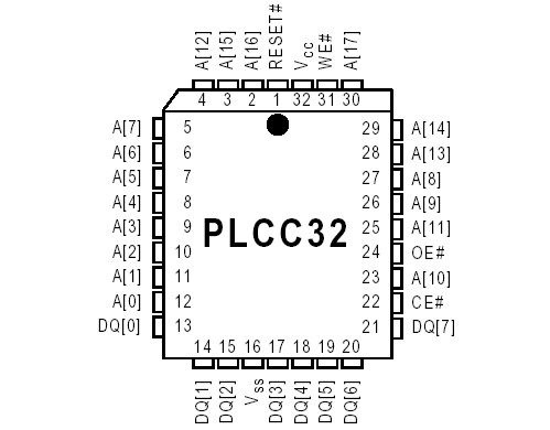
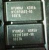
HY29F002T: Features: 5 Volt Read, Program, and Erase Minimizes system-level power requirementsHigh Performance Access times as fast as 45 nsLow Power Consumption 20 mA typical active read current 30 mA typ...

floor Price/Ceiling Price

Part Number:
HY29F002T
Supply Ability:
5000

Price Break

  • Qty
  • 1~5000
  • Unit Price
  • Negotiable
  • Processing time
  • 15 Days
Total Cost: $ 0.00

SeekIC Buyer Protection PLUS - newly updated for 2013!

  • Escrow Protection.
  • Guaranteed refunds.
  • Secure payments.
  • Learn more >>

Month Sales

268 Transactions

Rating

evaluate  (4.8 stars)

Upload time: 2024/5/3

Payment Methods

All payment methods are secure and covered by SeekIC Buyer Protection PLUS.

Notice: When you place an order, your payment is made to SeekIC and not to your seller. SeekIC only pays the seller after confirming you have received your order. We will also never share your payment details with your seller.
Product Details

Description


Features:

 5 Volt Read, Program, and Erase
   Minimizes system-level power requirements
 High Performance
   Access times as fast as 45 ns
 Low Power Consumption
   20 mA typical active read current
   30 mA typical program/erase current
   1 µA typical CMOS standby current
 Compatible with JEDEC Standards
   Package, pinout and command-set compatible with the single-supply Flash device standard
   Provides superior inadvertent write protection
 Sector Erase Architecture
   Boot sector architecture with top boot block location
   One 16 Kbyte, two 8 Kbyte, one 32 Kbyte and three 64K byte sectors
   A command can erase any combination of sectors
   Supports full chip erase
 Erase Suspend/Resume
   Temporarily suspends a sector erase operation to allow data to be read from, or programmed into, any sector not being erased
 Sector Protection
   Any combination of sectors may be locked to prevent program or erase operations within those sectors
 Temporary Sector Unprotect
   Allows changes in locked sectors (requires high voltage on RESET# pin)
 Internal Erase Algorithm
   Automatically erases a sector, any combination of sectors, or the entire chip
 Internal Programming Algorithm
   Automatically programs and verifies data at a specified address
 Fast Program and Erase Times
   Byte programming time: 7 µs typical
   Sector erase time: 1.0 sec typical
   Chip erase time: 7 sec typical
 Data# Polling and Toggle Status Bits
   Provide software confirmation of completion of program or erase operations
 Minimum 100,000 Program/Erase Cycles
 Space Efficient Packaging
   Available in industry-standard 32-pin TSOP and PLCC packages


Pinout

  Connection Diagram


Specifications

Symbol
Parametrics
Value
Unit
TSTG
Storage Temperature
-65 to +150
°C
TBIAS
Ambient Temperature with Power Applied
-55 to +125
°C
VIN2
Voltage on  pin with Respect VSS:
                 VCC1
                 A[9],OE#,RESET#2
                 All Other Pins1
-2.0 to +7.0
-2.0 to +12.5
-2.0 to +7.0
V
V
V
IOS
Output Short Circuit Current3
0 to +85
mA


Description

The HY29F002T is an 2 Megabit, 5 volt-only CMOS Flash memory organized as 262,144 (256K) bytes. The device is offered in industrystandard 32-pin TSOP and PLCC packages.

The HY29F002T can be programmed and erased in-system with a single 5-volt VCC supply. Internally generated and regulated voltages are provided for program and erase operations, so that the device does not require a high voltage power supply to perform those functions. The device can also be programmed in standard EPROM programmers. Access times as fast as 55ns over th full operating voltage range of 5.0 volts ± 10% are offered for timing compatibility with the zero wait state requirements of high speed microprocessors. A 45ns version operating over 5.0 volts ± 5% is also available. To eliminate bus contention, the HY29F002T has separate chip enable (CE#), write enable (WE#) and output enable (OE#) controls.

The device HY29F002T is compatible with the JEDEC single power-supply Flash command set standard. Commands are written to the command register using standard microprocessor write timings, from where they are routed to an internal state-machine that controls the erase and programming circuits. Device programming is performed a byte at a time by executing the four-cycle Program Command. This initiates an internal algorithm that automatically times the program pulse widths and verifies proper cell margin.

The HY29F002T's sector erase architecture allows any number of array sectors to be erased and reprogrammed without affecting the data contents of other sectors. Device erasure is initiated by executing the Erase Command. This initiates an internal algorithm that automatically preprograms the array (if it is not already programmed) before executing the erase operation. During erase cycles, the device automatically times the erase pulse widths and verifies proper cell margin.

To protect data in the device HY29F002T from accidental or unauthorized attempts to program or erase the device while it is in the system (e.g., by a virus), the device has a Sector Protect function which hardware write protects selected sectors. The sector protect and unprotect features can be enabled in a PROM programmer. Temporary Sector Unprotect, which requires a high voltage, allows in-system erasure and code changes in previously protected sectors.

Erase Suspend enables the user to put erase on hold for any period of time to read data from, or program data to, any sector that is not selected for erasure. True background erase can thus be achieved. The device HY29F002T is fully erased when shipped from the factory.

Addresses and data needed for the programming and erase operations are internally latched during write cycles, and the host system can detect completion of a program or erase operation by reading the DQ[7] (Data# Polling) and DQ[6] (toggle) status bits. Reading data from the device HY29F002T is similar to reading from SRAM or EPROM devices. Hardware data protection measures include a low VCC detector that automatically inhibits write operations during power transitions.

The host can place the device HY29F002T into the standby mode. Power consumption is greatly reduced in this mode.


Customers Who Bought This Item Also Bought

Margin,quality,low-cost products with low minimum orders. Secure your online payments with SeekIC Buyer Protection.
Integrated Circuits (ICs)
Cables, Wires
Hardware, Fasteners, Accessories
Cable Assemblies
Semiconductor Modules
Batteries, Chargers, Holders
View more