Features: • Maximum clock frequency up to 333 MHz
• Maximum data rate up to 666 Mbps/pin
• Data transfer on both edges of clock
• Programmable CAS latency of 2, 3 and 4 clocks
• Programmable burst length of 2, 4 and 8
• Integrated DLL to align DQS and DQ transitions with CLK
• Data transfer signals are synchronized with byte wise bidirectional Data Strobe
• Data Strobe signal edge-aligned with data for Read operations
• Data Strobe signal center aligned with data for Write operations
• Differential clock inputs (CLK and CLK)
• Data mask for masking write data, one DM per byte
• Organization 1024K * 32 * 4 banks
• 4096 rows and 256 columns per bank
• 4K Refresh (32ms)
• Refresh Interval 7.8 sec
• Autorefresh and Self Refresh available
• Standard JEDEC TF-XBGA 128 package
• Self-mirrored, symmetrical ball out
• Matched Impedance Mode interface (Z0=60)
• SSTL-2 JEDEC Weak Mode interface (Z0=34)
• IO voltage VDDQ = 2.5 V
• VDD power supply memory core:
Speed sorts 3 and 3.3: 2.5 V < VDD < 2.9 V
Speed sorts L4.5, 4.5, and 5: VDD = 2.5 V
Speed sorts L3.6 and 3.6 support both VDD modesSpecifications
| Parameter |
Symbol |
Values |
Unit |
Note/
Test Condition |
| min. |
typ. |
max. |
| Voltage on I/O pins relative to VSS |
VIN, VOUT |
0.5 |
- |
VDDQ +
0.5 |
V |
- |
| Voltage on Inputs relative to VSS |
VIN |
0.5 |
|
+3.6 |
V |
|
| Voltage on VDD supply relative to VSS |
VDD |
0.5 |
|
+3.6 |
V |
|
| Voltage on VDDQ supply relative to VSS |
VDDQ |
0.5 |
|
+3.6 |
V |
|
| Operating Temperature (Ambient) |
TA |
0 |
|
+70 |
°C |
|
| Storage Temperature (Plastic) |
TSTG |
55 |
|
+150 |
°C |
|
| Power Dissipation |
PD |
|
1.4 |
|
W |
|
| Short Circuit Output Current |
IOUT |
|
50 |
|
mA |
|
Attention: Stresses above those listed here may cause permanent damage to the device. Exposure to absolute maximum rating conditions for extended periods may affect device reliability.
Maximum ratings are absolute ratings; exceeding only one of these values may cause irreversible damage to the integrated circuit.
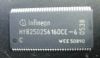
DescriptionThe Infineon 128Mbit DDR SGRAM HYB25D128323C-5 is a ultra high performance graphics memory device, designed to meet all requirements for high bandwidth intensive applications like PC graphics systems.
The 128Mbit DDR SGRAM HYB25D128323C-5 uses a double-data-rate DRAM architecture organized as 4 banks * 4096 rows * 256 columns * 32 bits. The double-data-rate architecture is essentially a 2n prefetch architecture, with an interface designed to transfer two data words per clock cycle at the I/O pins. A single Read or Write access to the DDRSGRAM consists of a single 64-bit wide, one clock cycle data transfer at the internal DRAM core and two corresponding 32-bit wide, one-half clock cycle data transfers at the I/O pins. The result is a data rate of 666 Mbits / sec per pin. The external data interface is 32 bit wide and achieves at 333 MHz system clock a peak bandwidth of 2.66 Gigabytes/sec.
The device HYB25D128323C-5 is supplied with 2.5 V resp. within the range of 2.5 V - 2.9 V for the memory core and 2.5 V for the output drivers. Two drivers strengths are available: 2.5 V Matched Impedance Mode and SSTL2 Weak Mode. The "Matched Impedance Mode" interface is optimized for high frequency digital data transfers and matches the impedance of graphics board systems (60Ohm).
Auto Refresh and Self Refresh operations are both supported.
A standard JEDEC TF-XBGA 128 package is used in HYB25D128323C-5 which enables ultra high speed clock and data transfer rates. The signals are mapped symmetrically to the balls in order to enable mirrored mounting in application.
The chip HYB25D128323C-5 is fabricated in Infineon technologies advanced 256M process technology.

 HYB25D128323C-5 Data Sheet